- 您现在的位置:买卖IC网 > PDF目录165343 > AD9753ASTZRL (ANALOG DEVICES INC) PARALLEL, WORD INPUT LOADING, 0.011 us SETTLING TIME, 12-BIT DAC, PQFP48 PDF资料下载
参数资料
| 型号: | AD9753ASTZRL |
| 厂商: | ANALOG DEVICES INC |
| 元件分类: | DAC |
| 英文描述: | PARALLEL, WORD INPUT LOADING, 0.011 us SETTLING TIME, 12-BIT DAC, PQFP48 |
| 封装: | 1.40 MM HEIGHT, ROHS COMPLIANT, PLASTIC, MS-026BBC, LQFP-48 |
| 文件页数: | 5/28页 |
| 文件大小: | 814K |
| 代理商: | AD9753ASTZRL |
第1页第2页第3页第4页当前第5页第6页第7页第8页第9页第10页第11页第12页第13页第14页第15页第16页第17页第18页第19页第20页第21页第22页第23页第24页第25页第26页第27页第28页
REV. B
AD9753
–13–
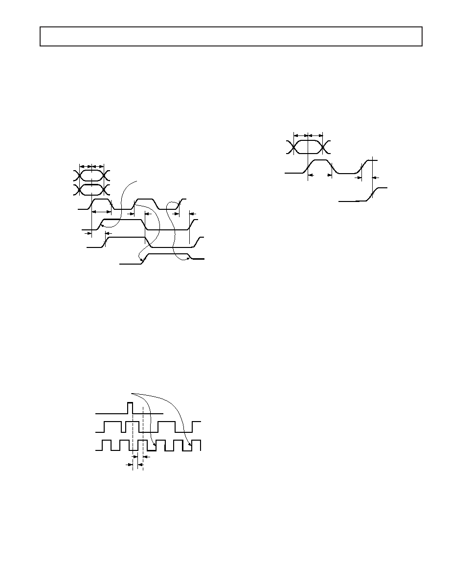
INTERLEAVED (2 ) MODE WITH PLL DISABLED
The relationship between the internal and external clocks in this
mode is shown in Figure 11. A clock at the output update data
rate (2
× the input data rate) must be applied to the CLK inputs.
Internal dividers then create the internal 1
× clock necessary for
the input latches. Although the input latches are updated on the
rising edge of the delayed internal 1
× clock, the setup-and-hold
times given in the Digital Specifications table are with respect to
the rising edge of the external 2
× clock. With the PLL disabled,
a load-dependent delayed version of the 1
× clock is present at
the PLLLOCK pin. This signal can be used to synchronize the
external data.
PORT 1
DATA X
DATA Y
tH
tS
tLPW
tPD
DATA X
DATA Y
PORT 2
IOUTA OR IOUTB
DELAYED
INTERNAL
1
CLK
DATA IN
tPD
tD
DATA ENTERS
INPUT LATCHES
ON THIS EDGE
EXTERNAL
2
CLK
EXTERNAL
1
CLK
@ PLLLOCK
Figure 11. Timing Requirements, Interleaved (2
×)
Mode with PLL Disabled
Updates to the data at input Ports 1 and 2 should be synchro-
nized to the specific rising edge of the external 2
× clock that
corresponds to the rising edge of the 1
× internal clock, as shown
in Figure 11. To ensure synchronization, a Logic 1 must be
momentarily applied to the RESET pin. Doing this and return-
ing RESET to Logic 0 brings the 1
× clock at PLLLOCK to a
Logic 1. On the next rising edge of the 2
× clock, the 1× clock
will go to Logic 0. On the second rising edge of the 2
× clock,
the 1
× clock (PLLLOCK) will again go to Logic 1, as well as
update the data in both of the input latches. The details of this
are shown in Figure 12.
RESET
PLLLOCK
EXTERNAL
2
CLOCK
tRH = 1.2ns
tRS = 0.2ns
DATA ENTERS
INPUT LATCHES
ON THESE EDGES
Figure 12. RESET Function Timing with PLL Disabled
For proper synchronization, sufficient delay must be present
between the time RESET goes low and the rising edge of the 2
×
clock. RESET going low must occur either at least tRS ns before
the rising edge of the 2
× clock, or t
RH ns afterwards. In the
first case, the immediately occurring CLK rising edge will
cause PLLLOCK to go low. In the second case, the next
CLK rising edge will toggle PLLLOCK.
NONINTERLEAVED MODE WITH PLL DISABLED
If the data at only one port is required, the AD9753 interface can
operate as a simple double buffered latch with no interleaving.
On the rising edge of the 1
× clock, input latch 1 or 2 is updated
with the present input data (depending on the state of DIV0/
DIV1). On the next rising edge, the DAC latch is updated and a
time tPD later, the DAC output reflects this change. Figure 13
represents the AD9753 timing in this mode.
tH
tS
tLPW
tPD
DATA OUT
PORT 1 OR
PORT 2
1
CLOCK
IOUTA OR IOUTB
XX
DATA IN
PORT 1 OR
PORT 2
Figure 13. Timing Requirements, Noninterleaved
Mode with PLL Disabled
DAC TRANSFER FUNCTION
The AD9753 provides complementary current outputs, IOUTA
and IOUTB. IOUTA will provide a near full-scale current output,
IOUTFS, when all bits are high (i.e., DAC CODE = 4095), while
IOUTB, the complementary output, provides no current. The
current output appearing at IOUTA and IOUTB is a function of
both the input code and IOUTFS and can be expressed as
IOUTA = (DAC CODE/4096)
× I
OUTFS
(1)
IOUTB = (4095 – DAC CODE)/4096
× IOUTFS
(2)
where DAC CODE = 0 to 4095 (i.e., decimal representation).
As mentioned previously, IOUTFS is a function of the reference
current, IREF, which is nominally set by a reference voltage,
VREFIO, and an external resistor RSET. It can be expressed as
IOUTFS = 32
× IREF
(3)
where
IREF = VREFIO/RSET
(4)
The two current outputs typically drive a resistive load directly
or via a transformer. If dc coupling is required, IOUTA and IOUTB
should be directly connected to matching resistive loads, RLOAD,
that are tied to analog common, ACOM. Note that RLOAD may
represent the equivalent load resistance seen by IOUTA or IOUTB
as would be the case in a doubly terminated 50
or 75 cable.
The single-ended voltage output appearing at the IOUTA and
IOUTB nodes is simply
VOUTA = IOUTA
× RLOAD
(5)
VOUTB = IOUTB
× R
LOAD
(6)
Note that the full-scale values of VOUTA and VOUTB should not
exceed the specified output compliance range to maintain
specified distortion and linearity performance.
VDIFF = (IOUTA – IOUTB)
× R
LOAD
(7)
相关PDF资料 |
PDF描述 |
|---|---|
| ADA123AL7 | FIBER OPTIC ADD/DROP MUX/DEMUX, LC/UPC CONNECTOR |
| ADA123AB1 | FIBER OPTIC ADD/DROP MUX/DEMUX, FC/PC CONNECTOR |
| ADA123AB2 | FIBER OPTIC ADD/DROP MUX/DEMUX, FC/APC CONNECTOR |
| ADA123AB4 | FIBER OPTIC ADD/DROP MUX/DEMUX, SC/APC CONNECTOR |
| ADA123AB6 | FIBER OPTIC ADD/DROP MUX/DEMUX, SC/SPC CONNECTOR |
相关代理商/技术参数 |
参数描述 |
|---|---|
| AD9753-EB | 功能描述:BOARD EVAL FOR AD9753 RoHS:否 类别:编程器,开发系统 >> 评估板 - 数模转换器 (DAC) 系列:TxDAC+® 产品培训模块:Lead (SnPb) Finish for COTS Obsolescence Mitigation Program 标准包装:1 系列:- DAC 的数量:4 位数:12 采样率(每秒):- 数据接口:串行,SPI? 设置时间:3µs DAC 型:电流/电压 工作温度:-40°C ~ 85°C 已供物品:板 已用 IC / 零件:MAX5581 |
| AD9754 | 制造商:AD 制造商全称:Analog Devices 功能描述:14-Bit, 125 MSPS High Performance TxDAC D/A Converter |
| AD9754AR | 功能描述:IC DAC 14BIT 125MSPS HP 28-SOIC RoHS:否 类别:集成电路 (IC) >> 数据采集 - 数模转换器 系列:TxDAC® 产品培训模块:Data Converter Fundamentals DAC Architectures 标准包装:750 系列:- 设置时间:7µs 位数:16 数据接口:并联 转换器数目:1 电压电源:双 ± 功率耗散(最大):100mW 工作温度:0°C ~ 70°C 安装类型:表面贴装 封装/外壳:28-LCC(J 形引线) 供应商设备封装:28-PLCC(11.51x11.51) 包装:带卷 (TR) 输出数目和类型:1 电压,单极;1 电压,双极 采样率(每秒):143k |
| AD9754ARRL | 制造商:Analog Devices 功能描述:DAC 1-CH 14-bit 28-Pin SOIC W T/R 制造商:Rochester Electronics LLC 功能描述:14-BIT, 125 MSPS+ TXDAC D/A CONVERTER - Tape and Reel |
发布紧急采购,3分钟左右您将得到回复。