- 您现在的位置:买卖IC网 > PDF目录17063 > AD9762-EBZ (Analog Devices Inc)BOARD EVAL FOR AD9762 PDF资料下载
参数资料
| 型号: | AD9762-EBZ |
| 厂商: | Analog Devices Inc |
| 文件页数: | 4/23页 |
| 文件大小: | 0K |
| 描述: | BOARD EVAL FOR AD9762 |
| 产品培训模块: | DAC Architectures |
| 标准包装: | 1 |
| 系列: | TxDAC® |
| DAC 的数量: | 1 |
| 位数: | 12 |
| 采样率(每秒): | 125M |
| 数据接口: | 并联 |
| 设置时间: | 35ns |
| DAC 型: | 电流 |
| 工作温度: | -40°C ~ 85°C |
| 已供物品: | 板 |
| 已用 IC / 零件: | AD9762 |
AD9762
–12–
REV. B
REFERENCE OPERATION
The AD9762 contains an internal 1.20 V bandgap reference
that can be easily disabled and overridden by an external refer-
ence. REFIO serves as either an input or output depending on
whether the internal or an external reference is selected. If
REFLO is tied to ACOM, as shown in Figure 40, the internal
reference is activated and REFIO provides a 1.20 V output. In
this case, the internal reference must be compensated externally
with a ceramic chip capacitor of 0.1
F or greater from REFIO
to REFLO. Also, REFIO should be buffered with an external
amplifier having an input bias current less than 100 nA if any
additional loading is required.
50pF
COMP1
+1.2V REF
AVDD
REFLO
CURRENT
SOURCE
ARRAY
0.1 F
+5V
REFIO
FS ADJ
2k
0.1 F
AD9762
ADDITIONAL
LOAD
OPTIONAL
EXTERNAL
REF BUFFER
Figure 40. Internal Reference Configuration
The internal reference can be disabled by connecting REFLO to
AVDD. In this case, an external reference may then be applied
to REFIO as shown in Figure 41. The external reference may
provide either a fixed reference voltage to enhance accuracy and
drift performance or a varying reference voltage for gain control.
Note that the 0.1
F compensation capacitor is not required
since the internal reference is disabled, and the high input
impedance (i.e., 1 M
) of REFIO minimizes any loading of the
external reference.
50pF
COMP1
+1.2V REF
AVDD
REFLO
CURRENT
SOURCE
ARRAY
0.1 F
AVDD
REFIO
FS ADJ
RSET
AD9762
EXTERNAL
REF
IREF =
VREFIO/RSET
AVDD
REFERENCE
CONTROL
AMPLIFIER
VREFIO
Figure 41. External Reference Configuration
REFERENCE CONTROL AMPLIFIER
The AD9762 also contains an internal control amplifier that is
used to regulate the DAC’s full-scale output current, IOUTFS.
The control amplifier is configured as a V-I converter as shown
in Figure 41, such that its current output, IREF, is determined by
the ratio of the VREFIO and an external resistor, RSET, as stated
in Equation 4. IREF is copied over to the segmented current
sources with the proper scaling factor to set IOUTFS as stated in
Equation 3.
The control amplifier allows a wide (10:1) adjustment span of
IOUTFS over a 2 mA to 20 mA range by setting IREF between
62.5
A and 625 A. The wide adjustment span of IOUTFS
provides several application benefits. The first benefit relates
directly to the power dissipation of the AD9762, which is
proportional to IOUTFS (refer to the Power Dissipation section).
The second benefit relates to the 20 dB adjustment, which is
useful for system gain control purposes.
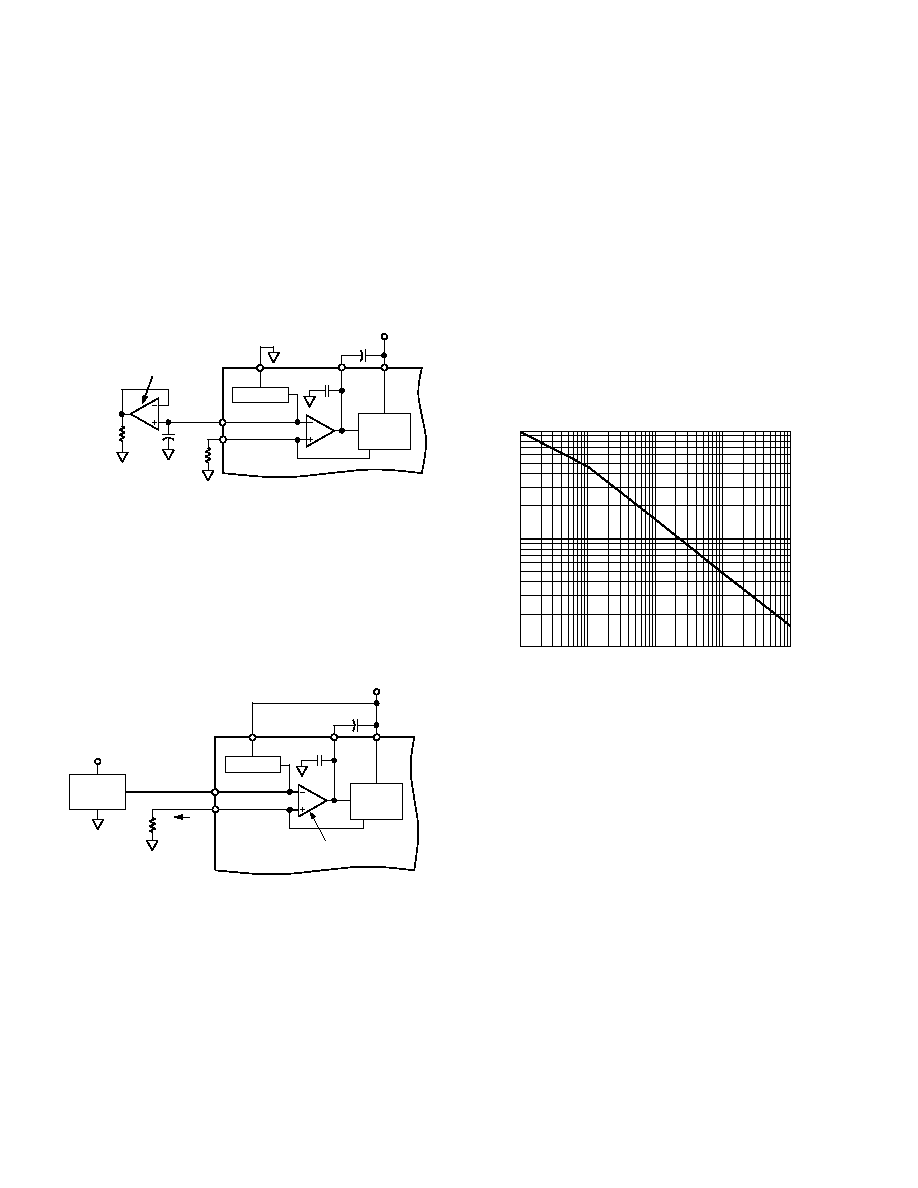
The small signal bandwidth of the reference control amplifier is
approximately 1.4 MHz and can be reduced by connecting an
external capacitor between COMP1 and AVDD. The output of
the control amplifier, COMP1, is internally compensated via a
50 pF capacitor that limits the control amplifier small-signal
bandwidth and reduces its output impedance. Any additional
external capacitance further limits the bandwidth and acts as a
filter to reduce the noise contribution from the reference ampli-
fier. Figure 42 shows the relationship between the external
capacitor and the small signal –3 dB bandwidth of the
COMP1 CAPACITOR – nF
1000
0.1
1000
BANDWIDTH
–
kHz
10
1
10
100
0
Figure 42. External COMP1 Capacitor vs. –3 dB Bandwidth
reference amplifier. Since the –3 dB bandwidth corresponds
to the dominant pole, and hence the time constant, the settling
time of the control amplifier to a stepped reference input
response can be approximated.
The optimum distortion performance for any reconstructed
waveform is obtained with a 0.1
F external capacitor installed.
Thus, if IREF is fixed for an application, a 0.1
F ceramic chip
capacitor is recommended. Also, since the control amplifier is
optimized for low power operation, multiplying applications
requiring large signal swings should consider using an external
control amplifier to enhance the application’s overall large signal
multiplying bandwidth and/or distortion performance.
There are two methods in which IREF can be varied for a fixed
RSET. The first method is suitable for a single-supply system in
which the internal reference is disabled, and the common-mode
voltage of REFIO is varied over its compliance range of 1.25 V
to 0.10 V. REFIO can be driven by a single-supply amplifier or
DAC, thus allowing IREF to be varied for a fixed RSET. Since the
input impedance of REFIO is approximately 1 M
, a simple,
low cost R-2R ladder DAC configured in the voltage mode
topology may be used to control the gain. This circuit is shown
in Figure 43 using the AD7524 and an external 1.2 V reference,
the AD1580.
相关PDF资料 |
PDF描述 |
|---|---|
| MIC2005-0.8YML TR | IC DISTRIBUTION SW 0.8A 6-MLF |
| AD9760-EBZ | BOARD EVAL FOR AD9760 |
| AD9748ACP-PCBZ | BOARD EVAL FOR AD9748ACP |
| GCM18DCTD-S288 | CONN EDGECARD 36POS .156 EXTEND |
| GBM24DSEI-S243 | CONN EDGECARD 48POS .156 EYELET |
相关代理商/技术参数 |
参数描述 |
|---|---|
| AD9763 | 制造商:AD 制造商全称:Analog Devices 功能描述:10-Bit, 125 MSPS Dual TxDAC+ D/A Converter |
| AD9763_11 | 制造商:AD 制造商全称:Analog Devices 功能描述:10-/12-/14-Bit, 125 MSPS Dual TxDAC Digital-to-Analog Converters |
| AD9763AST | 制造商:Analog Devices 功能描述:DAC 2-CH Segment 10-bit 48-Pin LQFP 制造商:Rochester Electronics LLC 功能描述:10 BIT, 125 MSPS DUAL TXDAC+ - Tape and Reel 制造商:Analog Devices 功能描述:IC 10-BIT DAC |
| AD9763ASTRL | 制造商:Analog Devices 功能描述:DAC 2-CH Segment 10-bit 48-Pin LQFP T/R 制造商:Rochester Electronics LLC 功能描述:10 BIT, 125 MSPS DUAL TXDAC+ - Tape and Reel |
| AD9763ASTZ | 功能描述:IC DAC 10BIT DUAL 125MSPS 48LQFP RoHS:是 类别:集成电路 (IC) >> 数据采集 - 数模转换器 系列:TxDAC+® 产品培训模块:Lead (SnPb) Finish for COTS Obsolescence Mitigation Program 标准包装:50 系列:- 设置时间:4µs 位数:12 数据接口:串行 转换器数目:2 电压电源:单电源 功率耗散(最大):- 工作温度:-40°C ~ 85°C 安装类型:表面贴装 封装/外壳:8-TSSOP,8-MSOP(0.118",3.00mm 宽) 供应商设备封装:8-uMAX 包装:管件 输出数目和类型:2 电压,单极 采样率(每秒):* 产品目录页面:1398 (CN2011-ZH PDF) |
发布紧急采购,3分钟左右您将得到回复。