参数资料
| 型号: | AD9764AR |
| 厂商: | Analog Devices Inc |
| 文件页数: | 3/22页 |
| 文件大小: | 0K |
| 描述: | IC DAC 14BIT 125MSPS 28-SOIC |
| 产品培训模块: | Data Converter Fundamentals DAC Architectures |
| 标准包装: | 27 |
| 系列: | TxDAC® |
| 设置时间: | 35ns |
| 位数: | 14 |
| 转换器数目: | 1 |
| 电压电源: | 模拟和数字 |
| 功率耗散(最大): | 170mW |
| 工作温度: | -40°C ~ 85°C |
| 安装类型: | 表面贴装 |
| 封装/外壳: | 28-SOIC(0.295",7.50mm 宽) |
| 供应商设备封装: | 28-SOIC W |
| 包装: | 管件 |
| 输出数目和类型: | 2 电流,单极;2 电流,双极 |
| 采样率(每秒): | 125M |
REV. B
AD9764
–11–
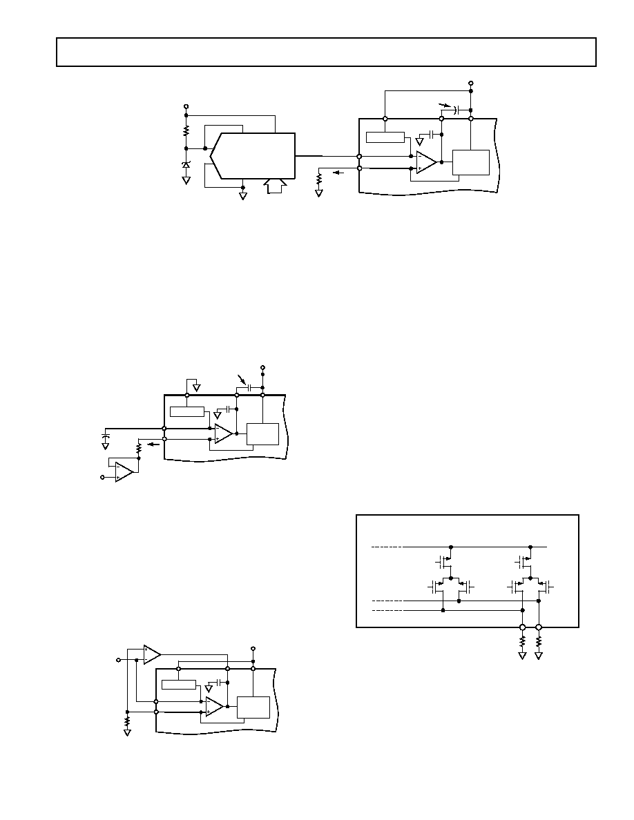
The second method may be used in a dual-supply system in
which the common-mode voltage of REFIO is fixed, and IREF is
varied by an external voltage, VGC, applied to RSET via an ampli-
fier. An example of this method is shown in Figure 26 in which
the internal reference is used to set the common-mode voltage
of the control amplifier to 1.20 V. The external voltage, VGC, is
referenced to ACOM and should not exceed 1.2 V. The value of
RSET is such that IREFMAX and IREFMIN do not exceed 62.5
A
and 625
A, respectively. The associated equations in Figure 26
can be used to determine the value of RSET.
50pF
COMP1 AVDD
REFLO
CURRENT
SOURCE
ARRAY
AVDD
REFIO
FS ADJ
RSET
AD9764
IREF
OPTIONAL
BANDLIMITING
CAPACITOR
VGC
1 F
IREF = (1.2–VGC)/RSET
WITH VGC < VREFIO AND 62.5 A
IREF
625A
+1.2V REF
Figure 26. Dual-Supply Gain Control Circuit
In some applications, the user may elect to use an external
control amplifier to enhance the multiplying bandwidth,
distortion performance and/or settling time. External amplifiers
capable of driving a 50 pF load such as the AD817 are suitable
for this purpose. It is configured in such a way that it is in
parallel with the weaker internal reference amplifier as shown in
Figure 27. In this case, the external amplifier simply overdrives
the weaker reference control amplifier. Also, since the internal
control amplifier has a limited current output, it will sustain no
damage if overdriven.
50pF
COMP1
+1.2V REF
AVDD
REFLO
CURRENT
SOURCE
ARRAY
AVDD
REFIO
FS ADJ
RSET
AD9764
VREF
INPUT
EXTERNAL
CONTROL AMPLIFIER
Figure 27. Configuring an External Reference Control
Amplifier
ANALOG OUTPUTS
The AD9764 produces two complementary current outputs,
IOUTA and IOUTB, which may be configured for single-end
or differential operation. IOUTA and IOUTB can be converted into
complementary single-ended voltage outputs, VOUTA and
VOUTB, via a load resistor, RLOAD, as described in the DAC
Transfer Function section by Equations 5 through 8. The
differential voltage, VDIFF, existing between VOUTA and VOUTB
can also be converted to a single-ended voltage via a transformer
or differential amplifier configuration.
Figure 28 shows the equivalent analog output circuit of the
AD9764 consisting of a parallel combination of PMOS differen-
tial current switches associated with each segmented current
source. The output impedance of IOUTA and IOUTB is determined
by the equivalent parallel combination of the PMOS switches
and is typically 100 k
in parallel with 5 pF. Due to the na-
ture of a PMOS device, the output impedance is also slightly
dependent on the output voltage (i.e., VOUTA and VOUTB) and, to
a lesser extent, the analog supply voltage, AVDD, and full-scale
current, IOUTFS. Although the output impedance’s signal depen-
dency can be a source of dc nonlinearity and ac linearity (i.e.,
distortion), its effects can be limited if certain precautions are
noted.
AD9764
AVDD
IOUTA
IOUTB
RLOAD
Figure 28. Equivalent Analog Output Circuit
IOUTA and IOUTB also have a negative and positive voltage compli-
ance range. The negative output compliance range of –1.0 V is
set by the breakdown limits of the CMOS process. Operation
beyond this maximum limit may result in a breakdown of the
output stage and affect the reliability of the AD9764. The posi-
tive output compliance range is slightly dependent on the full-
scale output current, IOUTFS. It degrades slightly from its nominal
1.2V
50pF
COMP1
+1.2V REF
AVDD
REFLO
CURRENT
SOURCE
ARRAY
AVDD
REFIO
FS ADJ
RSET
AD9764
IREF =
VREF/RSET
AVDD
OPTIONAL
BANDLIMITING
CAPACITOR
VREF
VDD
RFB
OUT1
OUT2
AGND
DB7–DB0
AD7524
AD1580
0.1V TO 1.2V
Figure 25. Single-Supply Gain Control Circuit
相关PDF资料 |
PDF描述 |
|---|---|
| AD9779BSVZ | IC DAC 16BIT DUAL 1GSPS 100TQFP |
| AD9786BSVZRL | IC DAC 16BIT INTERPOL/SP 80TQFP |
| AD9788BSVZRL | IC DAC 16BIT 800MSPS 100TQFP |
| AD9806KSTZ | IC CCD SIGNAL PROC 10BIT 48LQFP |
| AD9814JR | IC CCD SIGNAL PROC 14BIT 28-SOIC |
相关代理商/技术参数 |
参数描述 |
|---|---|
| AD9764ARRL | 功能描述:IC DAC 14BIT 125MSPS 28-SOIC RoHS:否 类别:集成电路 (IC) >> 数据采集 - 数模转换器 系列:TxDAC® 标准包装:47 系列:- 设置时间:2µs 位数:14 数据接口:并联 转换器数目:1 电压电源:单电源 功率耗散(最大):55µW 工作温度:-40°C ~ 85°C 安装类型:表面贴装 封装/外壳:28-SSOP(0.209",5.30mm 宽) 供应商设备封装:28-SSOP 包装:管件 输出数目和类型:1 电流,单极;1 电流,双极 采样率(每秒):* |
| AD9764ARU | 功能描述:IC DAC 14BIT 125MSPS 28-TSSOP RoHS:否 类别:集成电路 (IC) >> 数据采集 - 数模转换器 系列:TxDAC® 产品培训模块:Data Converter Fundamentals DAC Architectures 标准包装:750 系列:- 设置时间:7µs 位数:16 数据接口:并联 转换器数目:1 电压电源:双 ± 功率耗散(最大):100mW 工作温度:0°C ~ 70°C 安装类型:表面贴装 封装/外壳:28-LCC(J 形引线) 供应商设备封装:28-PLCC(11.51x11.51) 包装:带卷 (TR) 输出数目和类型:1 电压,单极;1 电压,双极 采样率(每秒):143k |
| AD9764ARURL | 功能描述:INTEGRATED CIRCUIT 制造商:analog devices inc. 系列:* 包装:带卷(TR) 零件状态:最後搶購 封装/外壳:28-TSSOP(0.173",4.40mm 宽) 供应商器件封装:28-TSSOP 标准包装:1 |
| AD9764ARURL7 | 功能描述:IC DAC 14BIT 125MSPS 28-TSSOP RoHS:否 类别:集成电路 (IC) >> 数据采集 - 数模转换器 系列:TxDAC® 标准包装:47 系列:- 设置时间:2µs 位数:14 数据接口:并联 转换器数目:1 电压电源:单电源 功率耗散(最大):55µW 工作温度:-40°C ~ 85°C 安装类型:表面贴装 封装/外壳:28-SSOP(0.209",5.30mm 宽) 供应商设备封装:28-SSOP 包装:管件 输出数目和类型:1 电流,单极;1 电流,双极 采样率(每秒):* |
| AD9764ARUZ | 功能描述:IC DAC 14BIT 125MSPS 28-TSSOP RoHS:是 类别:集成电路 (IC) >> 数据采集 - 数模转换器 系列:TxDAC® 产品培训模块:Lead (SnPb) Finish for COTS Obsolescence Mitigation Program 标准包装:50 系列:- 设置时间:4µs 位数:12 数据接口:串行 转换器数目:2 电压电源:单电源 功率耗散(最大):- 工作温度:-40°C ~ 85°C 安装类型:表面贴装 封装/外壳:8-TSSOP,8-MSOP(0.118",3.00mm 宽) 供应商设备封装:8-uMAX 包装:管件 输出数目和类型:2 电压,单极 采样率(每秒):* 产品目录页面:1398 (CN2011-ZH PDF) |
发布紧急采购,3分钟左右您将得到回复。