参数资料
| 型号: | AD9764ARUZ |
| 厂商: | Analog Devices Inc |
| 文件页数: | 7/22页 |
| 文件大小: | 0K |
| 描述: | IC DAC 14BIT 125MSPS 28-TSSOP |
| 产品培训模块: | Data Converter Fundamentals DAC Architectures |
| 标准包装: | 50 |
| 系列: | TxDAC® |
| 设置时间: | 35ns |
| 位数: | 14 |
| 转换器数目: | 1 |
| 电压电源: | 模拟和数字 |
| 功率耗散(最大): | 170mW |
| 工作温度: | -40°C ~ 85°C |
| 安装类型: | 表面贴装 |
| 封装/外壳: | 28-TSSOP(0.173",4.40mm 宽) |
| 供应商设备封装: | 28-TSSOP |
| 包装: | 管件 |
| 输出数目和类型: | 2 电流,单极;2 电流,双极 |
| 采样率(每秒): | 125M |
| 产品目录页面: | 785 (CN2011-ZH PDF) |
REV. B
AD9764
–15–
IOUTFS and RLOAD can be selected as long as the positive compli-
ance range is adhered to. One additional consideration in this
mode is the integral nonlinearity (INL) as discussed in the Ana-
log Output section of this data sheet. For optimum INL perfor-
mance, the single-ended, buffered voltage output configuration
is suggested.
AD9764
IOUTA
IOUTB 21
50
25
50
VOUTA = 0 TO +0.5V
IOUTFS = 20mA
22
Figure 36. 0 V to +0.5 V Unbuffered Voltage Output
SINGLE-ENDED BUFFERED VOLTAGE OUTPUT
CONFIGURATION
Figure 37 shows a buffered single-ended output configuration in
which the op amp U1 performs an I-V conversion on the
AD9764 output current. U1 maintains IOUTA (or IOUTB) at a
virtual ground, thus minimizing the nonlinear output impedance
effect on the DAC’s INL performance as discussed in the Ana-
log Output section. Although this single-ended configuration
typically provides the best dc linearity performance, its ac distor-
tion performance at higher DAC update rates may be limited by
U1’s slewing capabilities. U1 provides a negative unipolar
output voltage and its full-scale output voltage is simply the
product of RFB and IOUTFS. The full-scale output should be set
within U1’s voltage output swing capabilities by scaling IOUTFS
and/or RFB. An improvement in ac distortion performance may
result with a reduced IOUTFS since the signal current U1 will be
required to sink will be subsequently reduced.
AD9764
22
IOUTA
IOUTB 21
COPT
200
U1
VOUT = IOUTFS
RFB
IOUTFS = 10mA
RFB
200
Figure 37. Unipolar Buffered Voltage Output
POWER AND GROUNDING CONSIDERATIONS
In systems seeking to simultaneously achieve high speed and
high performance, the implementation and construction of the
printed circuit board design is often as important as the circuit
design. Proper RF techniques must be used in device selection,
placement and routing and supply bypassing and grounding.
Figures 42–47 illustrate the recommended printed circuit board
ground, power and signal plane layouts that are implemented on
the AD9764 evaluation board.
Proper grounding and decoupling should be a primary objective
in any high speed, high resolution system. The AD9764 features
separate analog and digital supply and ground pins to optimize
the management of analog and digital ground currents in a
system. In general, AVDD, the analog supply, should be decoupled
to ACOM, the analog common, as close to the chip as physi-
cally possible. Similarly, DVDD, the digital supply, should be
decoupled to DCOM as close as physically as possible.
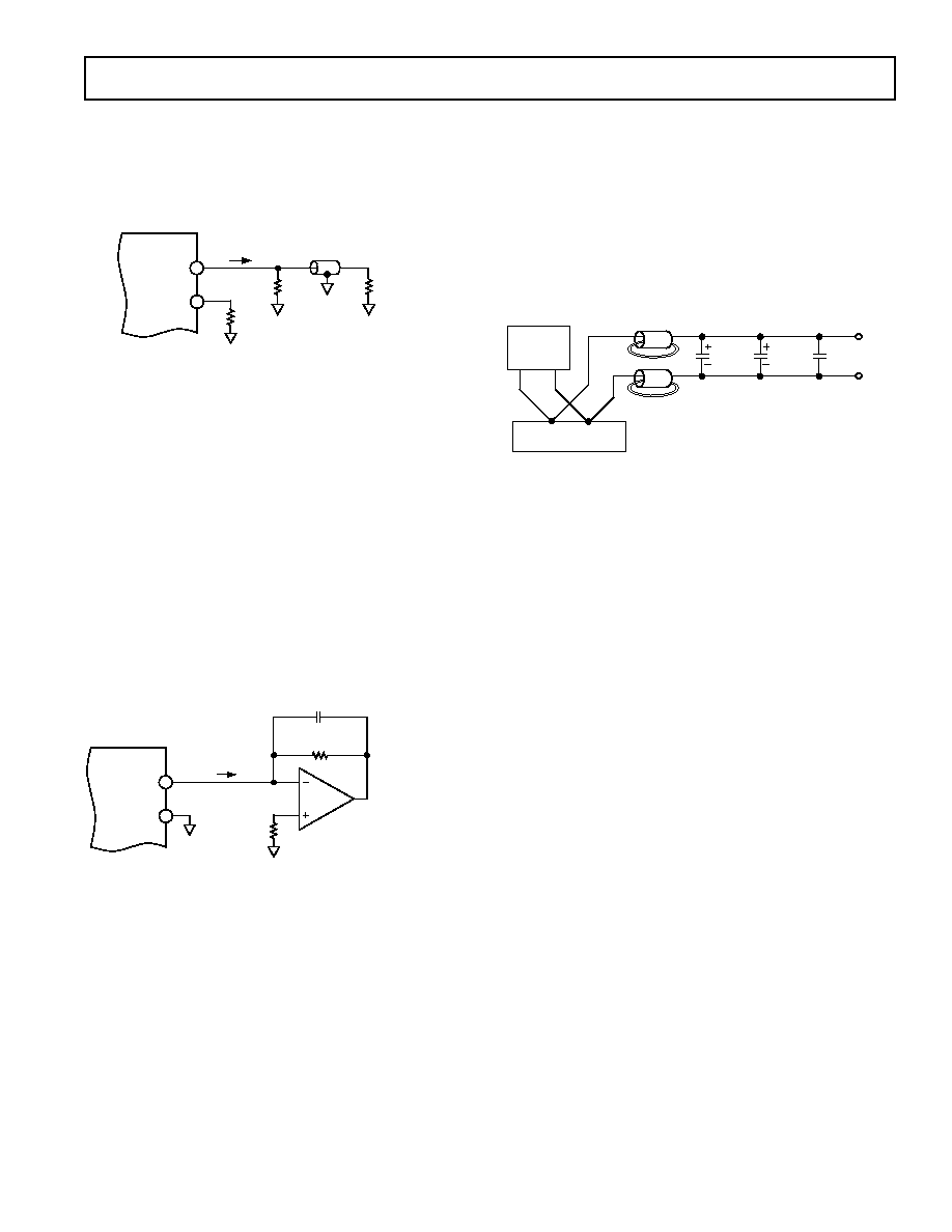
For those applications requiring a single +5 V or +3 V supply
for both the analog and digital supply, a clean analog supply
may be generated using the circuit shown in Figure 38. The
circuit consists of a differential LC filter with separate power
supply and return lines. Lower noise can be attained using low
ESR type electrolytic and tantalum capacitors.
100 F
ELECT.
10-22 F
TANT.
0.1 F
CER.
TTL/CMOS
LOGIC
CIRCUITS
+5V OR +3V
POWER SUPPLY
FERRITE
BEADS
AVDD
ACOM
Figure 38. Differential LC Filter for Single +5 V or +3 V
Applications
Maintaining low noise on power supplies and ground is critical
to obtain optimum results from the AD9764. If properly
implemented, ground planes can perform a host of functions on
high speed circuit boards: bypassing, shielding current trans-
port, etc. In mixed signal design, the analog and digital portions
of the board should be distinct from each other, with the analog
ground plane confined to the areas covering the analog signal
traces, and the digital ground plane confined to areas covering
the digital interconnects.
All analog ground pins of the DAC, reference and other analog
components should be tied directly to the analog ground plane.
The two ground planes should be connected by a path 1/8 to
1/4 inch wide underneath or within 1/2 inch of the DAC to
maintain optimum performance. Care should be taken to ensure
that the ground plane is uninterrupted over crucial signal paths.
On the digital side, this includes the digital input lines running
to the DAC as well as any clock signals. On the analog side, this
includes the DAC output signal, reference signal and the supply
feeders.
The use of wide runs or planes in the routing of power lines is
also recommended. This serves the dual role of providing a low
series impedance power supply to the part, as well as providing
some “free” capacitive decoupling to the appropriate ground
plane. It is essential that care be taken in the layout of signal and
power ground interconnects to avoid inducing extraneous volt-
age drops in the signal ground paths. It is recommended that all
connections be short, direct and as physically close to the pack-
age as possible in order to minimize the sharing of conduction
paths between different currents. When runs exceed an inch in
length, strip line techniques with proper termination resistors
should be considered. The necessity and value of this resistor
will be dependent upon the logic family used.
For a more detailed discussion of the implementation and con-
struction of high speed, mixed signal printed circuit boards,
refer to Analog Devices’ application notes AN-280 and AN-333.
相关PDF资料 |
PDF描述 |
|---|---|
| M83723/85G10056 | CONN RCPT 5POS JAM NUT W/PINS |
| VE-JTY-MZ-F4 | CONVERTER MOD DC/DC 3.3V 16.5W |
| ICS843004AGILFT | IC SYNTHESIZER LVPECL 24-TSSOP |
| LTC2614IGN-1#PBF | IC DAC 14BIT QUAD R-R 16-SSOP |
| MS3124E16-8S | CONN RCPT 8POS JAM NUT W/SCKT |
相关代理商/技术参数 |
参数描述 |
|---|---|
| AD9764ARUZRL7 | 功能描述:IC DAC 14BIT 125MSPS 28-TSSOP RoHS:是 类别:集成电路 (IC) >> 数据采集 - 数模转换器 系列:TxDAC® 标准包装:47 系列:- 设置时间:2µs 位数:14 数据接口:并联 转换器数目:1 电压电源:单电源 功率耗散(最大):55µW 工作温度:-40°C ~ 85°C 安装类型:表面贴装 封装/外壳:28-SSOP(0.209",5.30mm 宽) 供应商设备封装:28-SSOP 包装:管件 输出数目和类型:1 电流,单极;1 电流,双极 采样率(每秒):* |
| AD9764ARZ | 功能描述:IC DAC 14BIT 125MSPS 28-SOIC RoHS:是 类别:集成电路 (IC) >> 数据采集 - 数模转换器 系列:TxDAC® 产品培训模块:Lead (SnPb) Finish for COTS Obsolescence Mitigation Program 标准包装:50 系列:- 设置时间:4µs 位数:12 数据接口:串行 转换器数目:2 电压电源:单电源 功率耗散(最大):- 工作温度:-40°C ~ 85°C 安装类型:表面贴装 封装/外壳:8-TSSOP,8-MSOP(0.118",3.00mm 宽) 供应商设备封装:8-uMAX 包装:管件 输出数目和类型:2 电压,单极 采样率(每秒):* 产品目录页面:1398 (CN2011-ZH PDF) |
| AD9764ARZRL | 功能描述:IC DAC 14BIT 125MSPS 28SOIC RoHS:是 类别:集成电路 (IC) >> 数据采集 - 数模转换器 系列:TxDAC® 标准包装:47 系列:- 设置时间:2µs 位数:14 数据接口:并联 转换器数目:1 电压电源:单电源 功率耗散(最大):55µW 工作温度:-40°C ~ 85°C 安装类型:表面贴装 封装/外壳:28-SSOP(0.209",5.30mm 宽) 供应商设备封装:28-SSOP 包装:管件 输出数目和类型:1 电流,单极;1 电流,双极 采样率(每秒):* |
| AD9764-EB | 制造商:Analog Devices 功能描述: |
| AD9764-EBZ | 功能描述:BOARD EVAL FOR AD9764 RoHS:是 类别:编程器,开发系统 >> 评估板 - 数模转换器 (DAC) 系列:TxDAC® 产品培训模块:Lead (SnPb) Finish for COTS Obsolescence Mitigation Program 标准包装:1 系列:- DAC 的数量:4 位数:12 采样率(每秒):- 数据接口:串行,SPI? 设置时间:3µs DAC 型:电流/电压 工作温度:-40°C ~ 85°C 已供物品:板 已用 IC / 零件:MAX5581 |
发布紧急采购,3分钟左右您将得到回复。