参数资料
| 型号: | AD9779BSVZRL |
| 厂商: | Analog Devices Inc |
| 文件页数: | 18/56页 |
| 文件大小: | 0K |
| 描述: | IC DAC 16BIT DUAL 1GSPS 100TQFP |
| 产品培训模块: | Data Converter Fundamentals DAC Architectures |
| 标准包装: | 1,000 |
| 位数: | 16 |
| 数据接口: | 串行 |
| 转换器数目: | 2 |
| 电压电源: | 模拟和数字 |
| 功率耗散(最大): | 300mW |
| 工作温度: | -40°C ~ 85°C |
| 安装类型: | 表面贴装 |
| 封装/外壳: | 100-TQFP 裸露焊盘 |
| 供应商设备封装: | 100-TQFP-EP(14x14) |
| 包装: | 带卷 (TR) |
| 输出数目和类型: | 4 电流,单极 |
| 采样率(每秒): | 1G |
第1页第2页第3页第4页第5页第6页第7页第8页第9页第10页第11页第12页第13页第14页第15页第16页第17页当前第18页第19页第20页第21页第22页第23页第24页第25页第26页第27页第28页第29页第30页第31页第32页第33页第34页第35页第36页第37页第38页第39页第40页第41页第42页第43页第44页第45页第46页第47页第48页第49页第50页第51页第52页第53页第54页第55页第56页
AD9776/AD9778/AD9779
Rev. A | Page 25 of 56
THEORY OF OPERATION
The AD9776/AD9778/AD9779 combine many features that
make them very attractive DACs for wired and wireless
communications systems. The dual digital signal path and
dual DAC structure allow an easy interface with common
quadrature modulators when designing single sideband
transmitters. The speed and performance of the parts allow
wider bandwidths and more carriers to be synthesized than
in previously available DACs. The digital engine uses a break-
through filter architecture that combines the interpolation with
a digital quadrature modulator. This allows the parts to conduct
digital quadrature frequency upconversion. They also have
features that allow simplified synchronization with incoming
data and between multiple parts.
The serial port configuration is controlled by Register 0x00,
Bits<6:7>. It is important to note that the configuration changes
immediately upon writing to the last bit of the byte. For multi-
byte transfers, writing to this register can occur during the
middle of a communication cycle. Care must be taken to
compensate for this new configuration for the remaining bytes
of the current communication cycle.
The same considerations apply to setting the software reset,
RESET (Register 0x00, Bit 5) or pulling the RESET pin (Pin 70)
high. All registers are set to their default values, except
Register 0x00 and Register 0x04, which remain unchanged.
Use of only single-byte transfers when changing serial port
configurations or initiating a software reset is recommended to
prevent unexpected device behavior.
As described in this section, all serial port data is transferred
to/from the device in synchronization to the SCLK pin. If
synchronization is lost, the device has the ability to asynchro-
nously terminate an I/O operation, putting the serial port
controller into a known state and, thereby, regaining
synchronization.
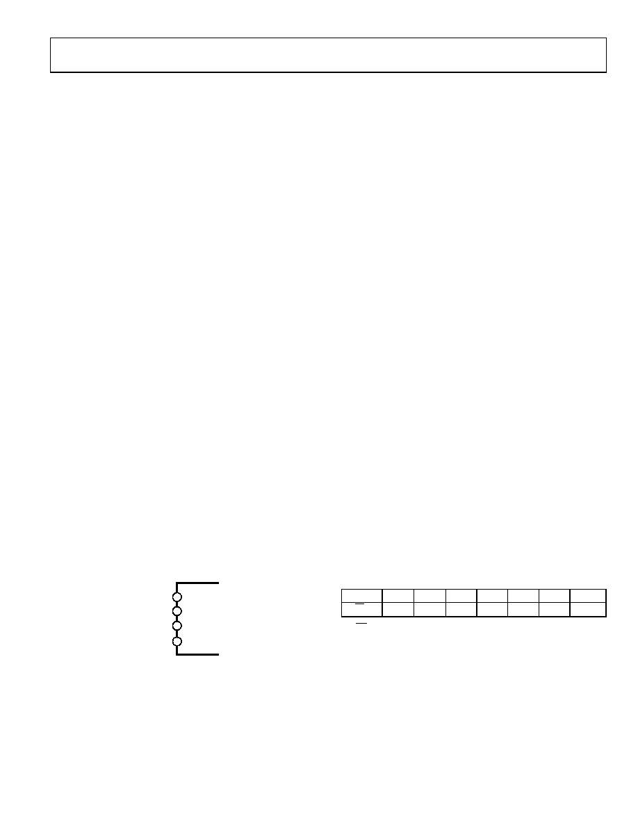
SERIAL PERIPHERAL INTERFACE
SPI_SDO
SPI
PORT
66
SPI_SDI 67
SPI_SCLK 68
SPI_CSB 69
05361-049
Figure 52. SPI Port
The serial port is a flexible, synchronous serial communications
port allowing easy interface to many industry-standard micro-
controllers and microprocessors. The serial I/O is compatible
with most synchronous transfer formats, including both the
Motorola SPI
and Intel SSR protocols. The interface allows
read/write access to all registers that configure the AD9776/
AD9778/AD9779. Single or multiple byte transfers are sup-
ported, as well as MSB-first or LSB-first transfer formats. The
serial interface ports can be configured as a single pin I/O (SDIO)
or two unidirectional pins for input/output (SDIO/SDO).
General Operation of the Serial Interface
There are two phases to a communication cycle with the
AD977x. Phase 1 is the instruction cycle (the writing of an
instruction byte into the device), coincident with the first eight
SCLK rising edges. The instruction byte provides the serial port
controller with information regarding the data transfer cycle,
Phase 2 of the communication cycle. The Phase 1 instruction
byte defines whether the upcoming data transfer is a read or
write, the number of bytes in the data transfer, and the starting
register address for the first byte of the data transfer. The first
eight SCLK rising edges of each communication cycle are used
to write the instruction byte into the device.
A logic high on the CSB pin followed by a logic low resets the
SPI port timing to the initial state of the instruction cycle.
From this state, the next eight rising SCLK edges represent the
instruction bits of the current I/O operation, regardless of the
state of the internal registers or the other signal levels at the
inputs to the SPI port. If the SPI port is in an instruction cycle
or a data transfer cycle, none of the present data is written.
The remaining SCLK edges are for Phase 2 of the communica-
tion cycle. Phase 2 is the actual data transfer between the device
and the system controller. Phase 2 of the communication cycle
is a transfer of one, two, three, or four data bytes as determined
by the instruction byte. Using one multibyte transfer is preferred.
Single-byte data transfers are useful in reducing CPU overhead
when register access requires only one byte. Registers change
immediately upon writing to the last bit of each transfer byte.
Instruction Byte
The instruction byte contains the information shown in
Table 9. SPI Instruction Byte
MSB
LSB
I7
I6
I5
I4
I3
I2
I1
I0
R/W
N1
N0
A4
A3
A2
A1
A0
R/W, Bit 7 of the instruction byte, determines whether a read or
a write data transfer occurs after the instruction byte write.
Logic high indicates a read operation. Logic 0 indicates a write
operation.
N1 and N0, Bit 6 and Bit 5 of the instruction byte, determine
the number of bytes to be transferred during the data transfer
cycle. The bit decodes are listed in Table 10.
A4, A3, A2, A1, and A0—Bit 4, Bit 3, Bit 2, Bit 1, and Bit 0, respec-
tively, of the instruction byte determine the register that is accessed
during the data transfer portion of the communication cycle.
相关PDF资料 |
PDF描述 |
|---|---|
| MAX9503GEEE+ | IC AMP VIDEO W/FILTER 16-QSOP |
| MAX9507ATE+ | IC DIRECTDRIVE FILTER AMP 16TQFN |
| AD7549JP | IC DAC 12BIT DUAL LC2MOS 20-PLCC |
| MAX9650AUA+ | IC OP AMP VCOM DRIVE 8-UMAX-EP |
| AD561JNZ | IC DAC 10BIT MONO VOLT IN 16DIP |
相关代理商/技术参数 |
参数描述 |
|---|---|
| AD9779BSVZRL1 | 制造商:AD 制造商全称:Analog Devices 功能描述:Dual 12-/14-/16-Bit, 1 GSPS, Digital-to-Analog Converters |
| AD9779-EB | 制造商:Analog Devices 功能描述:EVAL BOARD 16 BIT DUAL INTERPOLATION DAC - Bulk |
| AD9779-EBZ | 制造商:Analog Devices 功能描述:DUAL 16B, 1.0 GSPS TXDAC - Bulk |
| AD9779-EBZ1 | 制造商:AD 制造商全称:Analog Devices 功能描述:Dual 12-/14-/16-Bit, 1 GSPS, Digital-to-Analog Converters |
| AD9779PCB | 制造商:AD 制造商全称:Analog Devices 功能描述:Dual 16-Bit, 1.0 GSPS D/A Converter |
发布紧急采购,3分钟左右您将得到回复。