- 您现在的位置:买卖IC网 > PDF目录10068 > AD977AARZ (Analog Devices Inc)IC ADC 16BIT SRL 200KSPS 20SOIC PDF资料下载
参数资料
| 型号: | AD977AARZ |
| 厂商: | Analog Devices Inc |
| 文件页数: | 5/24页 |
| 文件大小: | 0K |
| 描述: | IC ADC 16BIT SRL 200KSPS 20SOIC |
| 标准包装: | 1 |
| 位数: | 16 |
| 采样率(每秒): | 200k |
| 数据接口: | 串行,SPI? |
| 转换器数目: | 1 |
| 功率耗散(最大): | 100mW |
| 电压电源: | 模拟和数字 |
| 工作温度: | -40°C ~ 85°C |
| 安装类型: | 表面贴装 |
| 封装/外壳: | 20-SOIC(0.295",7.50mm 宽) |
| 供应商设备封装: | 20-SOIC(宽型) |
| 包装: | 管件 |
| 输入数目和类型: | 3 个单端,单极;3 个单端,双极 |
AD977/AD977A
–13–
REV. D
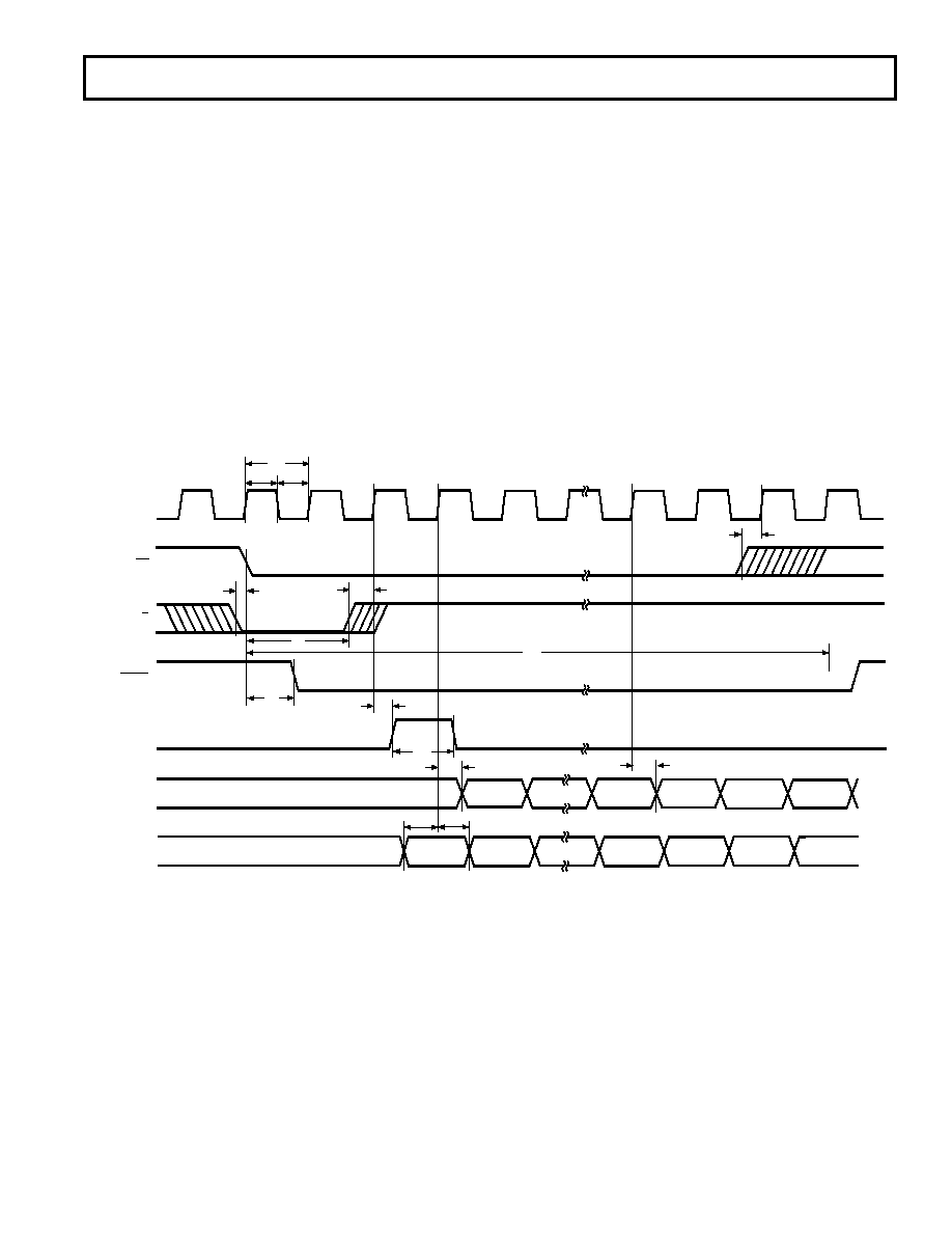
EXTERNAL CONTINUOUS CLOCK DATA READ DURING
CONVERSION WITH SYNC OUTPUT GENERATED
Figure 9 illustrates the method by which data from conversion
“n-1” can be read during conversion “n” while using a continu-
ous external clock with the generation of a SYNC output. What
permits the generation of a SYNC output is a transition of
DATACLK while either
CS is high or while both CS and R/C
are low.
With a continuous clock the
CS pin cannot be tied low as it
could be with a discontinuous clock. Use of a continuous clock
while a conversion is occurring can increase the DNL and
Transition Noise of the AD977/AD977A.
In Figure 9 a conversion is initiated by taking R/
C low with CS
held low. While this condition exists a transition of DATACLK,
clock pulse #0, will enable the generation of a SYNC pulse.
Less then 83 ns after R/
C is taken low the BUSY output will go
low to indicate that the conversion process has began. Figure 9
shows R/
C then going high and after a delay of greater than
15 ns (t15), clock pulse #1 can be taken high to request the
SYNC output. The SYNC output will appear approximately
50 ns after this rising edge and will be valid on the falling edge
of clock pulse #1 and the rising edge of clock pulse #2. The
MSB will be valid approximately 40 ns after the rising edge of
clock pulse #2 and can be latched off either the falling edge of
clock pulse #2 or the rising edge of clock pulse #3. The LSB
will be valid on the falling edge of clock pulse #17 and the rising
edge of clock pulse #18. Approximately 40 ns after the rising
edge of clock pulse #18, the DATA output pin will reflect the
state of the TAG input pin during the rising edge of clock
pulse #2.
For both the AD977 and the AD977A the data should be
clocked out during the 1st half of
BUSY so as not to degrade
conversion performance. For the AD977 this requires use of a
4.8 MHz DATACLK or greater with data being read out as
soon as the conversion process begins. For the AD977A it
requires use of a 10 MHz DATACLK or greater.
CS
BUSY
R/C
EXT
DATACLK
BIT 15
(MSB)
1
DATA
SYNC
03
BIT 0
(LSB)
TAG 0
TAG 1
TAG 0
TAG
2
t13
t14
t12
t19
18
t15
t16
t1
t20
t2
t17
t12
t18
t23
t24
t18
TAG 2
TAG 1
TAG 16
TAG 17
TAG 18
TAG 19
Figure 9. Conversion and Read Timing for Reading Previous Conversion Results During a Conversion Using An External
Continuous Data Clock (EXT/
INT Set to Logic High)
相关PDF资料 |
PDF描述 |
|---|---|
| MS27656T21B16PA | CONN RCPT 16POS WALL MNT W/PINS |
| IDT72241L15JI8 | IC FIFO 2048X18 SYNC 15NS 32PLCC |
| VI-B4Z-MV-F3 | CONVERTER MOD DC/DC 2V 60W |
| LT1080IN | IC DRVR/RCVR DUAL-RS232 5V 18DIP |
| AD977AAR | IC ADC 16BIT 200KSPS 20-SOIC |
相关代理商/技术参数 |
参数描述 |
|---|---|
| AD977AB2 | 制造商: 功能描述: 制造商:undefined 功能描述: |
| AD977ABN | 功能描述:IC ADC 16BIT 200KSPS 20-DIP RoHS:否 类别:集成电路 (IC) >> 数据采集 - 模数转换器 系列:- 标准包装:1 系列:- 位数:14 采样率(每秒):83k 数据接口:串行,并联 转换器数目:1 功率耗散(最大):95mW 电压电源:双 ± 工作温度:0°C ~ 70°C 安装类型:通孔 封装/外壳:28-DIP(0.600",15.24mm) 供应商设备封装:28-PDIP 包装:管件 输入数目和类型:1 个单端,双极 |
| AD977ABNZ | 功能描述:IC ADC 16BIT 200KSPS 20DIP RoHS:是 类别:集成电路 (IC) >> 数据采集 - 模数转换器 系列:- 产品培训模块:Lead (SnPb) Finish for COTS Obsolescence Mitigation Program 标准包装:2,500 系列:- 位数:12 采样率(每秒):3M 数据接口:- 转换器数目:- 功率耗散(最大):- 电压电源:- 工作温度:- 安装类型:表面贴装 封装/外壳:SOT-23-6 供应商设备封装:SOT-23-6 包装:带卷 (TR) 输入数目和类型:- |
| AD977ABR | 功能描述:IC ADC 16BIT 200KSPS 20-SOIC RoHS:否 类别:集成电路 (IC) >> 数据采集 - 模数转换器 系列:- 标准包装:1 系列:- 位数:14 采样率(每秒):83k 数据接口:串行,并联 转换器数目:1 功率耗散(最大):95mW 电压电源:双 ± 工作温度:0°C ~ 70°C 安装类型:通孔 封装/外壳:28-DIP(0.600",15.24mm) 供应商设备封装:28-PDIP 包装:管件 输入数目和类型:1 个单端,双极 |
| AD977ABRS | 功能描述:IC ADC 16BIT 200KSPS 28-SSOP RoHS:否 类别:集成电路 (IC) >> 数据采集 - 模数转换器 系列:- 标准包装:1 系列:- 位数:14 采样率(每秒):83k 数据接口:串行,并联 转换器数目:1 功率耗散(最大):95mW 电压电源:双 ± 工作温度:0°C ~ 70°C 安装类型:通孔 封装/外壳:28-DIP(0.600",15.24mm) 供应商设备封装:28-PDIP 包装:管件 输入数目和类型:1 个单端,双极 |
发布紧急采购,3分钟左右您将得到回复。