- 您现在的位置:买卖IC网 > PDF目录10517 > AD977ABRSZ (Analog Devices Inc)IC ADC 16BIT 200KSPS 28-SSOP PDF资料下载
参数资料
| 型号: | AD977ABRSZ |
| 厂商: | Analog Devices Inc |
| 文件页数: | 6/24页 |
| 文件大小: | 0K |
| 描述: | IC ADC 16BIT 200KSPS 28-SSOP |
| 标准包装: | 1 |
| 位数: | 16 |
| 采样率(每秒): | 200k |
| 数据接口: | 串行,SPI? |
| 转换器数目: | 1 |
| 功率耗散(最大): | 100mW |
| 电压电源: | 模拟和数字 |
| 工作温度: | -40°C ~ 85°C |
| 安装类型: | 表面贴装 |
| 封装/外壳: | 28-SSOP(0.209",5.30mm 宽) |
| 供应商设备封装: | 28-SSOP |
| 包装: | 管件 |
| 输入数目和类型: | 3 个单端,单极;3 个单端,双极 |
| 配用: | EVAL-AD977CB-ND - BOARD EVAL FOR AD977 EVAL-AD977ACB-ND - BOARD EVAL FOR AD977A |
AD977/AD977A
–14–
REV. D
Table I. AD977A Analog Input Configuration
Input Voltage
Connect R1IN
Connect R2IN
Connect R3IN
Input
Range
via 200
to
via 100
to
Impedance
±10 V
VIN
AGND
2.5 V
11.5 k
±5 V
AGND
VIN
2.5 V
6.7 k
±3.3 V
VIN
2.5 V
5.4 k
0 V to 10 V
AGND
VIN
AGND
6.7 k
0 V to 5 V
AGND
VIN
5.0 k
0 V to 4 V
VIN
AGND
VIN
5.4 k
Table II. AD977 Analog Input Configuration
Input Voltage
Connect R1IN
Connect R2IN
Connect R3IN
Input
Range
via 200
to
via 100
to
Impedance
±10 V
VIN
AGND
CAP
22.9 k
±5 V
AGND
VIN
CAP
13.3 k
±3.3 V
VIN
CAP
10.7 k
0 V to 10 V
AGND
VIN
AGND
13.3 k
0 V to 5 V
AGND
VIN
10.0 k
0 V to 4 V
VIN
AGND
VIN
10.7 k
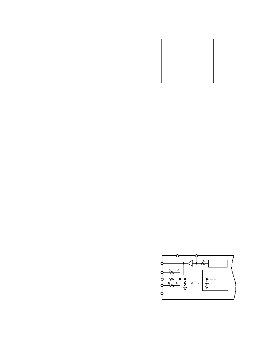
ANALOG INPUTS
The AD977/AD977A is specified to operate with six full-scale
analog input ranges. Connections required for each of the three
analog inputs, R1IN, R2IN and R3IN, and the resulting full-scale
ranges, are shown in Table I and Table II. The nominal input
impedance for each analog input range is also shown. Table III
shows the output codes for the ideal input voltages of each of the
six analog input ranges.
The analog input section has a
±25 V overvoltage protection on
R1IN and R2IN. Since the AD977/AD977A has two analog
grounds it is important to ensure that the analog input is refer-
enced to the AGND1 pin, the low current ground. This will
minimize any problems associated with a resistive ground drop.
It is also important to ensure that the analog input of the
AD977/AD977A is driven by a low impedance source. With its
primarily resistive analog input circuitry, the ADC can be driven
by a wide selection of general purpose amplifiers.
To best match the low distortion requirements of the AD977/
AD977A, care should be taken in the selection of the drive cir-
cuitry op amp.
Figure 10 shows the simplified analog input section for the
AD977/AD977A. Since the AD977/AD977A can operate with
an internal or external reference, and several different analog
input ranges, the full-scale analog input range is best represented
with a voltage that spans 0 V to VREF across the 40 pF sampling
capacitor. The onboard resistors are laser trimmed to ratio
match for adjustment of offset and full-scale error using fixed
external resistors.
The configurations shown in Figures 12 and 13 are required to
obtain the data sheet specifications for offset and full-scale error.
The external fixed resistors are used during factory calibration so
that a single 5 V supply can be used to bias the hardware trim
circuitry. With the hardware adjust circuits shown in Figures 12
and 13, offset and full-scale error can be trimmed to zero. Refer
to the Offset and Gain Adjust section.
If larger offset and full-scale errors are permitted, or if soft-
ware calibration is used, the external resistors can be omit-
ted. Table IV shows the resultant input ranges and offset and
full-scale errors.
Using the AD977A with Bipolar Input Ranges
The connection diagrams in Figure 11 show a buffer amplifier
required for bipolar operation of the AD977A when using the
internal reference. The buffer amplifier is required to isolate the
CAP pin from the signal dependent current in the R3IN pin. A
high speed op amp such as the AD8031 can be used with a
single 5 V power supply without degrading the performance of
the AD977A. The buffer must have good settling characteristics
and provide low total noise within the input bandwidth of the
AD977A.
R1IN
R2IN
R3IN
REF
4k
AGND2
CAP
AGND1
AD977/AD977A
20k /10k
2.5V
REFERENCE
10k /5k
5k /2.5k
20k /10k
40pF
SWITCHED
CAP ADC
Figure 10. AD977/AD977A Simplified Analog Input
相关PDF资料 |
PDF描述 |
|---|---|
| UP050B391K-KFC | CAP CER 390PF 50V 10% AXIAL |
| MAX3454EETE+ | IC TXRX USB ESD-PROT 16TQFN |
| SSM2019BRNZ | IC PREAMP AUDIO MONO AB 8SOIC |
| MAX3454EEUD+ | IC TXRX USB ESD-PROT 14TSSOP |
| UTS6JC106S | CONN PLUG CABLE 6X1.0 FEMALE |
相关代理商/技术参数 |
参数描述 |
|---|---|
| AD977ABRSZRL | 功能描述:IC ADC 16BIT 200KSPS 28SSOP RoHS:是 类别:集成电路 (IC) >> 数据采集 - 模数转换器 系列:- 标准包装:1 系列:- 位数:14 采样率(每秒):83k 数据接口:串行,并联 转换器数目:1 功率耗散(最大):95mW 电压电源:双 ± 工作温度:0°C ~ 70°C 安装类型:通孔 封装/外壳:28-DIP(0.600",15.24mm) 供应商设备封装:28-PDIP 包装:管件 输入数目和类型:1 个单端,双极 |
| AD977ABRZ | 功能描述:IC ADC 16BIT 200KSPS 20-SOIC RoHS:是 类别:集成电路 (IC) >> 数据采集 - 模数转换器 系列:- 标准包装:1 系列:microPOWER™ 位数:8 采样率(每秒):1M 数据接口:串行,SPI? 转换器数目:1 功率耗散(最大):- 电压电源:模拟和数字 工作温度:-40°C ~ 125°C 安装类型:表面贴装 封装/外壳:24-VFQFN 裸露焊盘 供应商设备封装:24-VQFN 裸露焊盘(4x4) 包装:Digi-Reel® 输入数目和类型:8 个单端,单极 产品目录页面:892 (CN2011-ZH PDF) 其它名称:296-25851-6 |
| AD977ACN | 制造商:Analog Devices 功能描述:ADC Single SAR 200ksps 16-bit Serial 20-Pin PDIP N 制造商:Rochester Electronics LLC 功能描述:200 KSPS 16-BIT ADC - Bulk |
| AD977ACNZ | 功能描述:IC ADC 16BIT 200KSPS 20DIP RoHS:是 类别:集成电路 (IC) >> 数据采集 - 模数转换器 系列:- 产品培训模块:Lead (SnPb) Finish for COTS Obsolescence Mitigation Program 标准包装:2,500 系列:- 位数:12 采样率(每秒):3M 数据接口:- 转换器数目:- 功率耗散(最大):- 电压电源:- 工作温度:- 安装类型:表面贴装 封装/外壳:SOT-23-6 供应商设备封装:SOT-23-6 包装:带卷 (TR) 输入数目和类型:- |
| AD977ACR | 功能描述:IC ADC 16BIT 200KSPS 20-SOIC RoHS:否 类别:集成电路 (IC) >> 数据采集 - 模数转换器 系列:- 产品培训模块:Lead (SnPb) Finish for COTS Obsolescence Mitigation Program 标准包装:2,500 系列:- 位数:12 采样率(每秒):3M 数据接口:- 转换器数目:- 功率耗散(最大):- 电压电源:- 工作温度:- 安装类型:表面贴装 封装/外壳:SOT-23-6 供应商设备封装:SOT-23-6 包装:带卷 (TR) 输入数目和类型:- |
发布紧急采购,3分钟左右您将得到回复。