- 您现在的位置:买卖IC网 > PDF目录10080 > AD977ACRZ (Analog Devices Inc)IC ADC 16BIT 200KSPS 20SOIC PDF资料下载
参数资料
| 型号: | AD977ACRZ |
| 厂商: | Analog Devices Inc |
| 文件页数: | 14/24页 |
| 文件大小: | 0K |
| 描述: | IC ADC 16BIT 200KSPS 20SOIC |
| 标准包装: | 1 |
| 位数: | 16 |
| 采样率(每秒): | 200k |
| 数据接口: | 串行,SPI? |
| 转换器数目: | 1 |
| 功率耗散(最大): | 100mW |
| 电压电源: | 模拟和数字 |
| 工作温度: | -40°C ~ 85°C |
| 安装类型: | 表面贴装 |
| 封装/外壳: | 20-SOIC(0.295",7.50mm 宽) |
| 供应商设备封装: | 20-SOIC W |
| 包装: | 管件 |
| 输入数目和类型: | 3 个单端,单极;3 个单端,双极 |
| 配用: | EVAL-AD977CB-ND - BOARD EVAL FOR AD977 EVAL-AD977ACB-ND - BOARD EVAL FOR AD977A |
AD977/AD977A
–21–
REV. D
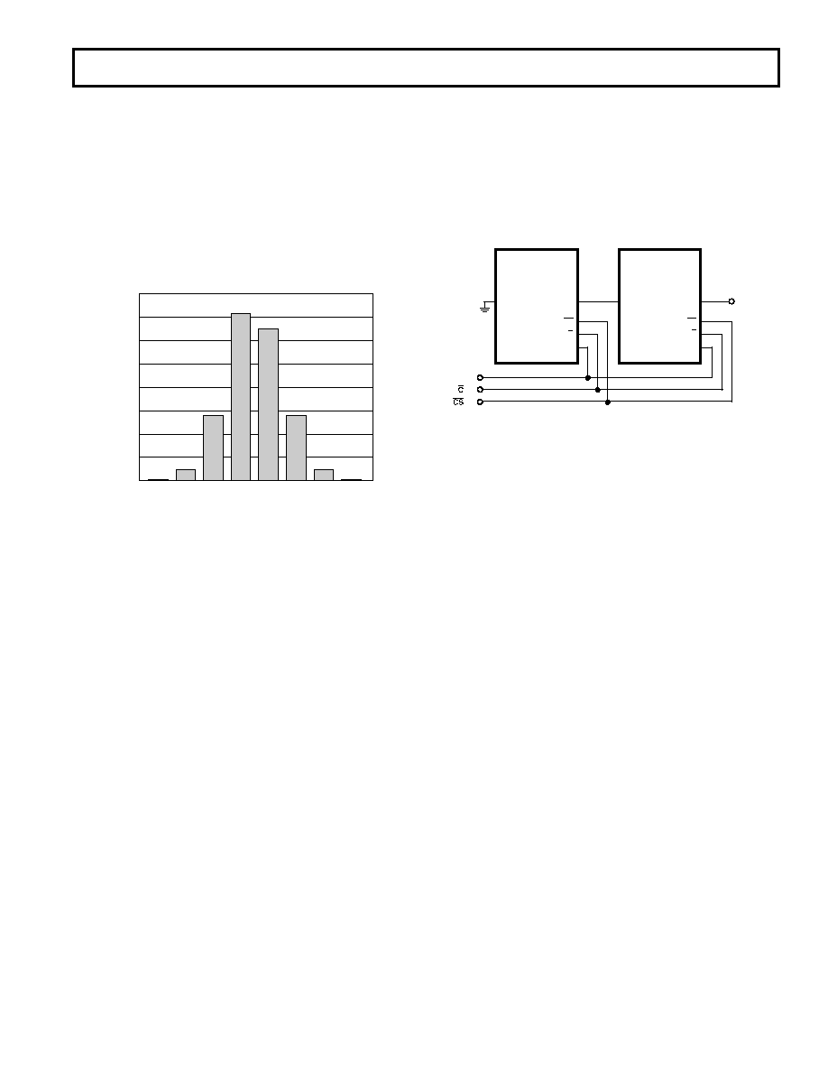
DC CODE UNCERTAINTY
Ideally, a fixed dc input should result in the same output code
for repetitive conversions; however, as a consequence of unavoid-
able circuit noise within the wideband circuits of the ADC, a
range of output codes may occur for a given input voltage.
Thus, when a dc signal is applied to the AD977/AD977A input
and 10,000 conversions are recorded, the result will be a distri-
bution of codes as shown in Figure 26. This histogram shows a
bell shaped curve consistent with the Gaussian nature of thermal
noise. The histogram is approximately seven codes wide. The
standard deviation of this Gaussian distribution results in a code
transition noise of 1 LSB rms.
4000
3500
0
–3
2000
1500
1000
500
3000
2500
–2
–10
1
2
3
4
Figure 26. Histogram of 10,000 Conversions of a DC Input
USE OF THE TAG INPUT
The AD977/AD977A provides a TAG input pin for cascading
multiple converters together. This feature is useful for reducing
component count in systems where an isolation barrier must be
crossed and is also useful for systems with a limited capacity for
interfacing to a large number of converters.
The tag feature only works in the external clock mode and
requires that the DATA output of a “upstream” device be con-
nected to the TAG input of an “downstream” device.
An example of the concatenation of two devices is shown in
Figure 27 and their resultant output is shown in Figure 28.
In Figure 27, the paralleled R/
C ensures that each AD977/
AD977A will simultaneously sample their inputs. In Figure 28,
a “null” bit is shown between each 16-bit word associated with
each ADC in the serial data output stream. This is the result of
a minimum value for “External Data Clock to Data Valid Delay”
(t18) that is greater than the “TAG Valid Setup Time” (t23). In
other words, when you concatenate two or more AD977/AD977As
the MSB on the downstream device will not be present on the
TAG input of the upstream device in time to meet the setup
time requirement of the TAG input.
If the serial data stream is going to a parallel port of a micro-
processor that is also providing the serial data clock, then the
microprocessor’s firmware can be written to “throw away” the
null bit. If the serial data stream is going to a serial port then
external “glue” logic will have to be added to make the interface
work. If the serial port has a “sync” input then this can be used
to throw away the null bit if the sync input is toggled each time
the null bit appears.
If the application does not require simultaneous sampling, the
null bit can be completely avoided by delaying the R/
C signal
of each upstream device by one clock cycle with respect to its
immediate downstream device. This bit time delay can be accom-
plished through a D-type flip-flop that delays the R/
C signal at
its D-input by one cycle of the serial data clock that is at its
clock input.
DATA OUT
DCLK IN
R/
IN
TAG
DATA
DCLK
AD977/AD977A
#2
(UPSTREAM)
AD977/AD977A
#1
(DOWNSTREAM)
TAG
DATA
DCLK
CS
R/C
CS
R/C
Figure 27. Two AD977/AD977A’s Utilizing Tag
It is not recommended that the TAG feature be used with the
read during convert mode because this will require data to be
clocked out during the second half of the conversion process. It
is recommended that the read after convert mode be used in an
application that wants to take advantage of the TAG feature. To
improve the data throughput a combination of the two data read
methods can be used and is described as follows.
If two or more AD977/AD977As are to have their data output
concatenated together in a single data stream, and if data
throughput is to be maximized, a system could be designed such
that the upstream device data is read during the first half of its
conversion process and the remainder of the downstream devices
read during the time between conversions. Assume three AD977As
are to have their data concatenated. Assume the further most
downstream device is referred to as device #1 and the further
most upstream device as #3. Each device is driven from a com-
mon DATACLK and R/
C control signal, the CS input of each
device is tied to ground. The three
BUSY outputs should be
OR’d together to form a composite
BUSY. After the conversion
is complete, as indicated by the composite
BUSY going high, an
external, normally low, 15.15 MHz DATACLK can be toggled
34 times to first read the data first from device #3 and then
from device #2. When the composite BUSY goes low to indicate
the beginning of the conversion process the external DATA-
CLK can be toggled 17 times to read the data from device #1
during the first half of the conversion process. Using this tech-
nique it would be possible to read in the data from the three
devices in approximately 6.4
s for a throughput of approxi-
mately 156 kHz The receiving device would have to deal with
the null bit between data from device #2 and #3. The receiving
device would also have to be capable of starting and stopping
the external DATACLK at the appropriate times.
The TAG input, when unused, should always be tied either high
or low and not be allowed to float.
相关PDF资料 |
PDF描述 |
|---|---|
| LTC2863HS8-1#TRPBF | IC TRANSCEIVER RS485 8-SOIC |
| LTC2863HDD-2#TRPBF | IC TRANSCEIVER RS485 8-DFN |
| AD977BRRL | IC ADC 16BIT 100KSPS 20-SOIC |
| VE-24P-IU-F1 | CONVERTER MOD DC/DC 13.8V 200W |
| AD976AR | IC ADC 16BIT 100KSPS 28-SOIC |
相关代理商/技术参数 |
参数描述 |
|---|---|
| AD977AN | 功能描述:IC ADC 16BIT 100KSPS 20-DIP RoHS:否 类别:集成电路 (IC) >> 数据采集 - 模数转换器 系列:- 标准包装:1 系列:- 位数:14 采样率(每秒):83k 数据接口:串行,并联 转换器数目:1 功率耗散(最大):95mW 电压电源:双 ± 工作温度:0°C ~ 70°C 安装类型:通孔 封装/外壳:28-DIP(0.600",15.24mm) 供应商设备封装:28-PDIP 包装:管件 输入数目和类型:1 个单端,双极 |
| AD977ANZ | 功能描述:IC ADC 16BIT 100KSPS 20-DIP RoHS:是 类别:集成电路 (IC) >> 数据采集 - 模数转换器 系列:- 标准包装:1 系列:microPOWER™ 位数:8 采样率(每秒):1M 数据接口:串行,SPI? 转换器数目:1 功率耗散(最大):- 电压电源:模拟和数字 工作温度:-40°C ~ 125°C 安装类型:表面贴装 封装/外壳:24-VFQFN 裸露焊盘 供应商设备封装:24-VQFN 裸露焊盘(4x4) 包装:Digi-Reel® 输入数目和类型:8 个单端,单极 产品目录页面:892 (CN2011-ZH PDF) 其它名称:296-25851-6 |
| AD977AR | 功能描述:IC ADC 16BIT 100KSPS 20-SOIC RoHS:否 类别:集成电路 (IC) >> 数据采集 - 模数转换器 系列:- 标准包装:1 系列:- 位数:14 采样率(每秒):83k 数据接口:串行,并联 转换器数目:1 功率耗散(最大):95mW 电压电源:双 ± 工作温度:0°C ~ 70°C 安装类型:通孔 封装/外壳:28-DIP(0.600",15.24mm) 供应商设备封装:28-PDIP 包装:管件 输入数目和类型:1 个单端,双极 |
| AD977AR-REEL | 功能描述:IC ADC 16BIT 100KSPS 20-SOIC RoHS:否 类别:集成电路 (IC) >> 数据采集 - 模数转换器 系列:- 标准包装:1 系列:- 位数:14 采样率(每秒):83k 数据接口:串行,并联 转换器数目:1 功率耗散(最大):95mW 电压电源:双 ± 工作温度:0°C ~ 70°C 安装类型:通孔 封装/外壳:28-DIP(0.600",15.24mm) 供应商设备封装:28-PDIP 包装:管件 输入数目和类型:1 个单端,双极 |
| AD977ARS | 功能描述:IC ADC 16BIT 100KSPS 28-SSOP RoHS:否 类别:集成电路 (IC) >> 数据采集 - 模数转换器 系列:- 标准包装:1 系列:- 位数:14 采样率(每秒):83k 数据接口:串行,并联 转换器数目:1 功率耗散(最大):95mW 电压电源:双 ± 工作温度:0°C ~ 70°C 安装类型:通孔 封装/外壳:28-DIP(0.600",15.24mm) 供应商设备封装:28-PDIP 包装:管件 输入数目和类型:1 个单端,双极 |
发布紧急采购,3分钟左右您将得到回复。