- 您现在的位置:买卖IC网 > PDF目录10118 > AD977CRZ (Analog Devices Inc)IC ADC 16BIT 100KSPS 20SOIC PDF资料下载
参数资料
| 型号: | AD977CRZ |
| 厂商: | Analog Devices Inc |
| 文件页数: | 15/24页 |
| 文件大小: | 0K |
| 描述: | IC ADC 16BIT 100KSPS 20SOIC |
| 标准包装: | 1 |
| 位数: | 16 |
| 采样率(每秒): | 100k |
| 数据接口: | 串行,SPI? |
| 转换器数目: | 1 |
| 功率耗散(最大): | 100mW |
| 电压电源: | 模拟和数字 |
| 工作温度: | -40°C ~ 85°C |
| 安装类型: | 表面贴装 |
| 封装/外壳: | 20-SOIC(0.295",7.50mm 宽) |
| 供应商设备封装: | 20-SOIC W |
| 包装: | 管件 |
| 输入数目和类型: | 3 个单端,单极;3 个单端,双极 |
| 配用: | EVAL-AD977CB-ND - BOARD EVAL FOR AD977 EVAL-AD977ACB-ND - BOARD EVAL FOR AD977A |
AD977/AD977A
–22–
REV. D
DATA
NULL BIT
DEVICE DATA #1
DEVICE
DATA #2
15
0
15
DCLK
R/
C
BUSY
Figure 28. TAG Timing Diagram for Two Concatenated
AD977/AD977As
POWER-DOWN FEATURE
The AD977/AD977A has analog and reference power-down
capability through the PWRD pin. When the PWRD pin is
taken high, the power consumption drops from a maximum
value of 100 mW to a typical value of 50
W. When in the
power-down mode the previous conversion results are still avail-
able in the internal registers and can be read out providing it has
not already been shifted out.
When used with an external reference, connected to the REF
pin and a 2.2
F capacitor, connected to the CAP pin, the
power up recovery time is typically 1 ms. This typical value of
1 ms for recovery time depends on how much charge has decayed
from the external 2.2
F capacitor on the CAP pin and assumes
that it has decayed to zero. The 1 ms recovery time has been
specified such that settling to 16-bits has been achieved.
When used with the internal reference, the dominant time con-
stant for power-up recovery is determined by the external
capacitor on the REF pin and the internal 4K impedance seen
at that pin. An external 2.2
F capacitor is recommended for the
REF pin.
CONSIDERATIONS WHEN USING MULTIPLEXED
INPUTS
Consideration must be given to the effect on A/D performance
in applications that require the use of analog multiplexers or analog
switches to interface multiple signals to the AD977/AD977A. The
nonzero “on” resistance of a multiplexer or switch, at the input
to the AD977/AD977A, will increase the system offset and gain
error. As an example, consider the AD977 configured for an input
voltage range of
±10 V dc. For every 5 of source impedance
(in addition to the required external 200
input resistor) an
offset error of 1 LSB would be introduced and the positive
gain error would increase by an added 0.00375% of full scale.
This error, due to nonzero source impedance, can be cor-
rected through a hardware or software system level calibration,
but will only be valid at the temperature and input voltage
present at the time of calibration. Another factor to consider is
that most analog multiplexers and switches exhibit a nonlinear
relationship between input signal level and on resistance. This
will introduce added distortion products that will degrade THD,
S/(N+D) and INL. For these reasons it is recommended that an
appropriate buffer be used between the output of the multiplexer
and the input of the AD977.
When switching the input to the multiplexer, and subsequently
the input to the AD977, it is recommended that the transition
be made to occur either immediately after the current conver-
sion is complete or shortly after the beginning of a conversion.
MICROPROCESSOR INTERFACING
The AD977/AD977A is ideally suited for traditional dc mea-
surement applications supporting a microprocessor, and ac
signal processing applications interfacing to a digital signal
processor. The AD977/AD977A is designed to interface with a
general purpose serial port or I/O ports on a microcontroller. A
variety of external buffers can be used with the AD977/AD977A
to prevent digital noise from coupling into the ADC. The
following sections illustrate the use of the AD977/AD977A with
an SPI equipped microcontroller and the ADSP-2181 signal
processor.
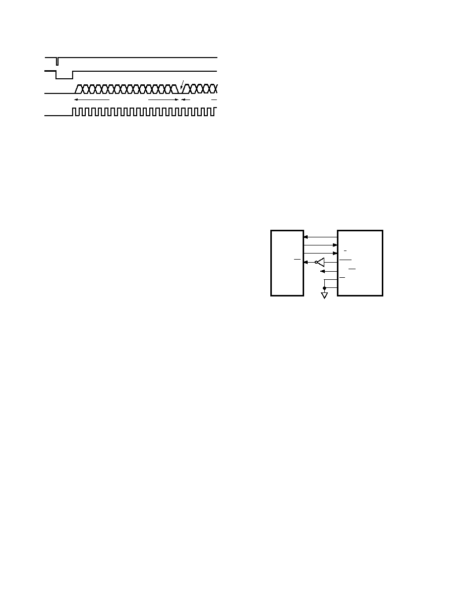
SPI Interface
Figure 29 shows a general interface diagram between the
AD977/AD977A and an SPI equipped microcontroller. This
interface assumes that the convert pulses will originate from the
microcontroller and that the AD977/AD977A will act as the
slave device. The convert pulse could be initiated in response to
an internal timer interrupt. The reading of output data, one byte
at a time, if necessary, could be initiated in response to the end-
of-conversion signal (
BUSY going high).
+5V
SDI
SCK
I/O PORT
IRQ
SPI
DATACLK
DATA
TAG
AD977/
AD977A
EXT/INT
CS
BUSY
R/C
Figure 29. AD977/AD977A to SPI Interface
ADSP-2181 Interface
Figure 30 shows an interface between the AD977/AD977A and
the ADSP-2181 Digital Signal Processor. The AD977/AD977A
is configured for the Internal Clock mode (EXT/
INT = 0) and
will therefore act as the master device. The convert command is
shown generated from an external oscillator in order to provide
a low jitter signal appropriate for both dc and ac measurements.
Because the SPORT, within the ADSP-2181, will be seeing a
discontinuous external clock, some steps are required to ensure
that the serial port is properly synchronized to this clock during
each data read operation. The recommended procedure to ensure
this is as follows,
– enable SPORT0 through the System Control register
– set the SCLK Divide register to zero
– setup PF0 and PF1 as outputs by setting bits 0 and 1 in
PFTYPE
– force RFS0 low through PF0. The Receive Frame Sync signal
has been programmed active high
– enable AD977/AD977A by forcing
CS = 0 through PF1
– enable SPORT0 Receive Interrupt through the IMASK register
– wait for at least one full conversion cycle of the AD977/AD977A
and throw away the received data
– disable the AD977/AD977A by forcing
CS = 1 through PF1
– wait for a period of time equal to one conversion cycle
– force RFS0 high through PF0
– enable the AD977/AD977A by forcing
CS = 0 through PF1
相关PDF资料 |
PDF描述 |
|---|---|
| VI-2NR-MX-F1 | CONVERTER MOD DC/DC 7.5V 75W |
| AD7892ANZ-1 | IC ADC 12BIT LP 500KSPS 24DIP |
| VI-2NP-MX-F4 | CONVERTER MOD DC/DC 13.8V 75W |
| AD7892ANZ-3 | IC ADC 12BIT LP 600KSPS 24DIP |
| MS27656T19B35P | CONN RCPT 66POS WALL MNT W/PINS |
相关代理商/技术参数 |
参数描述 |
|---|---|
| AD977CRZRL | 功能描述:IC ADC 16BIT 100KSPS 20SOIC RoHS:是 类别:集成电路 (IC) >> 数据采集 - 模数转换器 系列:- 标准包装:1,000 系列:- 位数:12 采样率(每秒):300k 数据接口:并联 转换器数目:1 功率耗散(最大):75mW 电压电源:单电源 工作温度:0°C ~ 70°C 安装类型:表面贴装 封装/外壳:24-SOIC(0.295",7.50mm 宽) 供应商设备封装:24-SOIC 包装:带卷 (TR) 输入数目和类型:1 个单端,单极;1 个单端,双极 |
| AD9780 | 制造商:AD 制造商全称:Analog Devices 功能描述:Dual 12-/14-/16-Bit, LVDS Interface, 500 MSPS DACs |
| AD9780BCPZ | 功能描述:IC DAC 12BT 600MSPS LVDS 72LFCSP RoHS:是 类别:集成电路 (IC) >> 数据采集 - 数模转换器 系列:- 产品培训模块:Data Converter Fundamentals DAC Architectures 标准包装:750 系列:- 设置时间:7µs 位数:16 数据接口:并联 转换器数目:1 电压电源:双 ± 功率耗散(最大):100mW 工作温度:0°C ~ 70°C 安装类型:表面贴装 封装/外壳:28-LCC(J 形引线) 供应商设备封装:28-PLCC(11.51x11.51) 包装:带卷 (TR) 输出数目和类型:1 电压,单极;1 电压,双极 采样率(每秒):143k |
| AD9780BCPZRL | 功能描述:IC DAC 12BT 600MSPS LVDS 72LFCSP RoHS:是 类别:集成电路 (IC) >> 数据采集 - 数模转换器 系列:- 产品培训模块:Data Converter Fundamentals DAC Architectures 标准包装:750 系列:- 设置时间:7µs 位数:16 数据接口:并联 转换器数目:1 电压电源:双 ± 功率耗散(最大):100mW 工作温度:0°C ~ 70°C 安装类型:表面贴装 封装/外壳:28-LCC(J 形引线) 供应商设备封装:28-PLCC(11.51x11.51) 包装:带卷 (TR) 输出数目和类型:1 电压,单极;1 电压,双极 采样率(每秒):143k |
| AD9780-EBZ | 制造商:Analog Devices 功能描述:EVAL BD FOR AD9780 DGTL-TO-ANLG CNVRTR - Bulk |
发布紧急采购,3分钟左右您将得到回复。