- 您现在的位置:买卖IC网 > PDF目录10977 > AD9833BRMZ-REEL (Analog Devices Inc)IC WAVEFORM GEN PROG 10MSOP PDF资料下载
参数资料
| 型号: | AD9833BRMZ-REEL |
| 厂商: | Analog Devices Inc |
| 文件页数: | 5/24页 |
| 文件大小: | 0K |
| 描述: | IC WAVEFORM GEN PROG 10MSOP |
| 产品培训模块: | Direct Digital Synthesis Tutorial Series (1 of 7): Introduction Direct Digital Synthesizer Tutorial Series (7 of 7): DDS in Action Direct Digital Synthesis Tutorial Series (3 of 7): Angle to Amplitude Converter Direct Digital Synthesis Tutorial Series (6 of 7): SINC Envelope Correction Direct Digital Synthesis Tutorial Series (4 of 7): Digital-to-Analog Converter Direct Digital Synthesis Tutorial Series (2 of 7): The Accumulator |
| 标准包装: | 3,000 |
| 分辨率(位): | 10 b |
| 主 fclk: | 25MHz |
| 调节字宽(位): | 28 b |
| 电源电压: | 2.3 V ~ 5.5 V |
| 工作温度: | -40°C ~ 105°C |
| 安装类型: | 表面贴装 |
| 封装/外壳: | 10-TFSOP,10-MSOP(0.118",3.00mm 宽) |
| 供应商设备封装: | 10-MSOP |
| 包装: | 带卷 (TR) |
Data Sheet
AD9833
Rev. E | Page 13 of 24
FUNCTIONAL DESCRIPTION
SERIAL INTERFACE
The AD9833 has a standard 3-wire serial interface that is
compatible with the SPI, QSPI, MICROWIRE, and DSP
interface standards.
Data is loaded into the device as a 16-bit word under the
control of a serial clock input, SCLK. The timing diagram for
this operation is given in .
The FSYNC input is a level-triggered input that acts as a frame
synchronization and chip enable. Data can be transferred into the
device only when FSYNC is low. To start the serial data transfer,
FSYNC should be taken low, observing the minimum FSYNC-
to-SCLK falling edge setup time, t7. After FSYNC goes low, serial
data is shifted into the input shift register of the device on the
falling edges of SCLK for 16 clock pulses. FSYNC may be taken
high after the 16th falling edge of SCLK, observing the minimum
SCLK falling edge to FSYNC rising edge time, t8. Alternatively,
FSYNC can be kept low for a multiple of 16 SCLK pulses and
then brought high at the end of the data transfer. In this way, a
continuous stream of 16-bit words can be loaded while FSYNC
is held low; FSYNC goes high only after the 16th SCLK falling
edge of the last word loaded.
The SCLK can be continuous, or it can idle high or low between
write operations. In either case, it must be high when FSYNC
goes low (t11).
For an example of how to program the AD9833, see the AN-1070
Application Note on the Analog Devices, Inc., website.
POWERING UP THE AD9833
The flowchart in Figure 26 shows the operating routine for the
AD9833. When the AD9833 is powered up, the part should be
reset. This resets the appropriate internal registers to 0 to provide
an analog output of midscale.
To avoid spurious DAC outputs during AD9833 initialization,
the reset bit should be set to 1 until the part is ready to begin
generating an output. A reset does not reset the phase, frequency,
or control registers. These registers will contain invalid data and,
therefore, should be set to known values by the user. The reset
bit should then be set to 0 to begin generating an output. The
data appears on the DAC output seven or eight MCLK cycles
after the reset bit is set to 0.
LATENCY PERIOD
A latency period is associated with each asynchronous write
operation in the AD9833. If a selected frequency or phase
register is loaded with a new word, there is a delay of seven
or eight MCLK cycles before the analog output changes. The
delay can be seven or eight cycles, depending on the position
of the MCLK rising edge when the data is loaded into the
destination register.
CONTROL REGISTER
The AD9833 contains a 16-bit control register that allows the
user to configure the operation of the AD9833. All control bits
other than the mode bit are sampled on the internal falling edge
of MCLK.
Table 6 describes the individual bits of the control register.
The different functions and the various output options of
the AD9833 are described in more detail in the Frequency and
Phase Registers section.
To inform the AD9833 that the contents of the control register
will be altered, D15 and D14 must be set to 0, as shown in Table 5.
Table 5. Control Register Bits
D15
D14
D13
D0
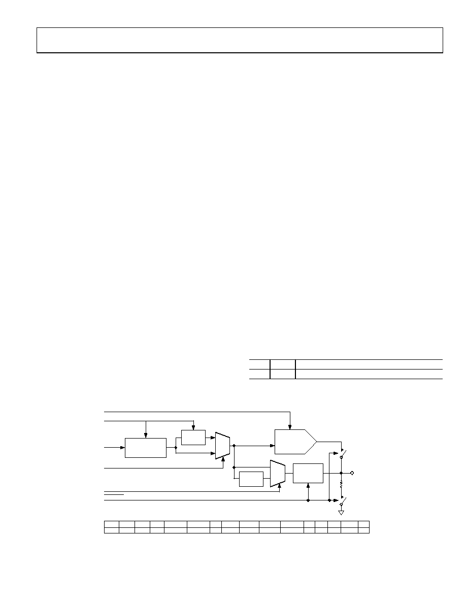
0
Control Bits
SIN
ROM
PHASE
ACCUMULATOR
(28-BIT)
AD9833
(LOW POWER)
10-BIT DAC
0
MUX
1
SLEEP12
SLEEP1
RESET
MODE + OPBITEN
DIV2
OPBITEN
VOUT
1
MUX
0
DIGITAL
OUTPUT
(ENABLE)
DIVIDE
BY 2
DB15
0
DB14
0
DB13
B28
DB12
HLB
DB11
FSELECT
DB10
PSELECT
DB9
0
DB8
RESET
DB7
SLEEP1
DB6
SLEEP12
DB5
OPBITEN
DB4
0
DB3
DIV2
DB2
0
DB1
MODE
DB0
0
02704-
024
Figure 24. Function of Control Bits
相关PDF资料 |
PDF描述 |
|---|---|
| MCF51AC128ACPUE | MCU 32BIT 128K FLASH CAN 64-LQFP |
| VE-B1B-IX-B1 | CONVERTER MOD DC/DC 95V 75W |
| VE-B14-IX-B1 | CONVERTER MOD DC/DC 48V 75W |
| VE-21D-CU-S | CONVERTER MOD DC/DC 85V 200W |
| VE-21B-CU-S | CONVERTER MOD DC/DC 95V 200W |
相关代理商/技术参数 |
参数描述 |
|---|---|
| AD9833BRMZ-REEL7 | 功能描述:IC WAVEFORM GEN PROG 10MSOP RoHS:是 类别:集成电路 (IC) >> 接口 - 直接数字合成 (DDS) 系列:- 产品变化通告:Product Discontinuance 27/Oct/2011 标准包装:2,500 系列:- 分辨率(位):10 b 主 fclk:25MHz 调节字宽(位):32 b 电源电压:2.97 V ~ 5.5 V 工作温度:-40°C ~ 85°C 安装类型:表面贴装 封装/外壳:16-TSSOP(0.173",4.40mm 宽) 供应商设备封装:16-TSSOP 包装:带卷 (TR) |
| AD9833SRMZ-EP-RL7 | 制造商:Analog Devices 功能描述:10 bit 10 pin DDS I.C. |
| AD9833WBRMZ-REEL | 制造商:Analog Devices 功能描述:10 BIT, 10 PIN DDS I.C. - Tape and Reel |
| AD9834 | 制造商:AD 制造商全称:Analog Devices 功能描述:Low Power, +2.3 V to +5.5 V, 50 MHz Complete DDS |
| AD9834_10 | 制造商:AD 制造商全称:Analog Devices 功能描述:20 mW Power, 2.3 V to 5.5 V,75 MHz Complete DDS |
发布紧急采购,3分钟左右您将得到回复。