- 您现在的位置:买卖IC网 > PDF目录10978 > AD9835BRUZ-REEL7 (Analog Devices Inc)IC DDS 10BIT 50MHZ 16-TSSOP PDF资料下载
参数资料
| 型号: | AD9835BRUZ-REEL7 |
| 厂商: | Analog Devices Inc |
| 文件页数: | 14/28页 |
| 文件大小: | 0K |
| 描述: | IC DDS 10BIT 50MHZ 16-TSSOP |
| 产品培训模块: | Direct Digital Synthesis Tutorial Series (1 of 7): Introduction Direct Digital Synthesizer Tutorial Series (7 of 7): DDS in Action Direct Digital Synthesis Tutorial Series (3 of 7): Angle to Amplitude Converter Direct Digital Synthesis Tutorial Series (6 of 7): SINC Envelope Correction Direct Digital Synthesis Tutorial Series (4 of 7): Digital-to-Analog Converter Direct Digital Synthesis Tutorial Series (2 of 7): The Accumulator |
| 标准包装: | 1,000 |
| 分辨率(位): | 10 b |
| 主 fclk: | 50MHz |
| 调节字宽(位): | 32 b |
| 电源电压: | 4.75 V ~ 5.25 V |
| 工作温度: | -40°C ~ 85°C |
| 安装类型: | 表面贴装 |
| 封装/外壳: | 16-TSSOP(0.173",4.40mm 宽) |
| 供应商设备封装: | 16-TSSOP |
| 包装: | 带卷 (TR) |
| 配用: | EVAL-AD9835EBZ-ND - BOARD EVALUATION FOR AD9835 |
第1页第2页第3页第4页第5页第6页第7页第8页第9页第10页第11页第12页第13页当前第14页第15页第16页第17页第18页第19页第20页第21页第22页第23页第24页第25页第26页第27页第28页
Data Sheet
AD9835
Rev. A | Page 21 of 28
AD9835-TO-68HC11/68L11 INTERFACE
the 68HC11/68L11 microcontroller. The microcontroller is
configured as the master by setting bit MSTR in the SPCR to 1
and, this provides a serial clock on SCK while the MOSI output
drives the serial data line SDATA. Since the microcontroller
does not have a dedicated frame sync pin, the FSYNC signal is
derived from a port line (PC7). The setup conditions for correct
operation of the interface are as follows: the SCK idles high
between write operations (CPOL = 0), data is valid on the SCK
falling edge (CPHA = 1). When data is being transmitted to the
AD9835, the FSYNC line is taken low (PC7). Serial data from
the 68HC11/68L11 is transmitted in 8-bit bytes with only eight
falling clock edges occurring in the transmit cycle. Data is
transmitted MSB first. In order to load data into the AD9835, PC7
is held low after the first eight bits are transferred and a second
serial write operation is performed to the AD9835. Only after
the second eight bits have been transferred should FSYNC be
taken high again.
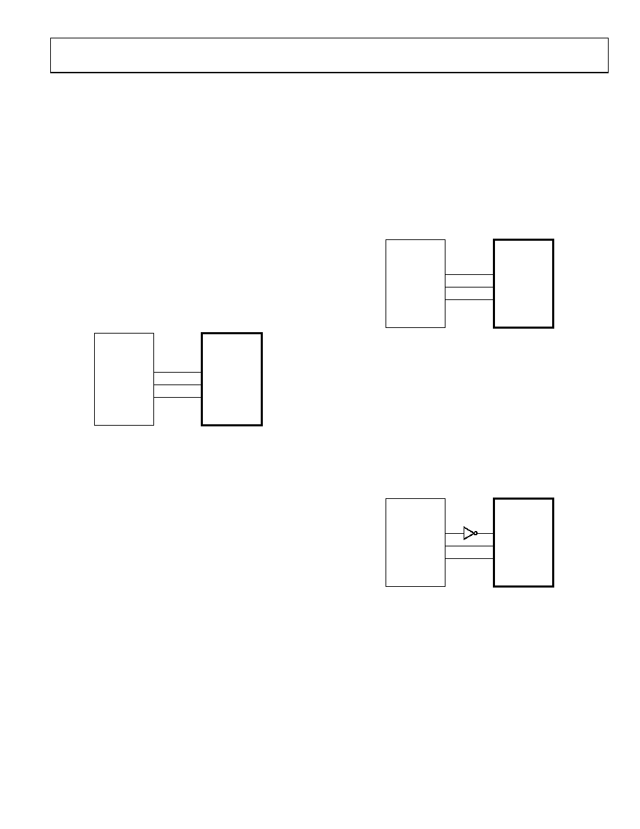
AD9835*
FSYNC
SDATA
SCLK
68HC11/68L11*
PC7
MOSI
SCK
*ADDITIONAL PINS OMITTED FOR CLARITY.
09
63
0-
0
29
Figure 27. 68HC11/68L11-to-AD9835 Interface
AD9835-TO-80C51/80L51 INTERFACE
the 80C51/80L51 microcontroller. The microcontroller is
operated in Mode 0 so that TXD of the 80C51/80L51 drives
SCLK of the AD9835 while RXD drives the serial data line
SDATA. The FSYNC signal is again derived from a bit
programmable pin on the port (P3.3 being used in the
diagram). When data is to be transmitted to the AAD9835,
P3.3 is taken low. The 80C51/80L51 transmits data in 8-bit
bytes thus, only eight falling SCLK edges occur in each cycle.
To load the remaining eight bits to the AD9835, P3.3 is held
low after the first eight bits have been transmitted and a second
write operation is initiated to transmit the second byte of data.
P3.3 is taken high following the completion of the second write
operation. SCLK should idle high between the two write
operations. The 80C51/ 80L51 outputs the serial data in a
format which has the LSB first. The AD9835 accepts the MSB
first (the 4 MSBs being the control information, the next 4 bits
being the address while the 8 LSBs contain the data when
writing to a destination register). Therefore, the transmit
routine of the 80C51/80L51 must take this into account and
rearrange the bits so that the MSB is output first.
AD9835*
FSYNC
SDATA
SCLK
80C51/80L51*
P3.3
RxD
TxD
*ADDITIONAL PINS OMITTED FOR CLARITY.
09
63
0-
0
30
Figure 28. 80C51/80L51 to AD9835 Interface
AD9835-TO-DSP56002 INTERFACE
DSP56002. The DSP56002 is configured for normal mode
asynchronous operation with a gated internal clock (SYN = 0,
GCK = 1, SCKD = 1). The frame sync pin is generated internally
(SC2 = 1), the transfers are 16 bits wide (WL1 = 1, WL0 = 0)
and the frame sync signal will frame the 16 bits (FSL = 0).
The frame sync signal is available on pin SC2 but, it needs to be
inverted before being applied to the AD9835. The interface to
the DSP56000/DSP56001 is similar to that of the DSP56002.
AD9835*
FSYNC
SDATA
SCLK
DSP56002*
SC2
STD
SCK
*ADDITIONAL PINS OMITTED FOR CLARITY.
09
63
0-
0
31
Figure 29. AD9835-to-DSP56002 Interface
相关PDF资料 |
PDF描述 |
|---|---|
| AD9835BRUZ-REEL | IC DDS 10BIT 50MHZ 16-TSSOP |
| VE-BWX-IX-B1 | CONVERTER MOD DC/DC 5.2V 75W |
| VI-B1F-IX-B1 | CONVERTER MOD DC/DC 72V 75W |
| VI-B1F-IW-B1 | CONVERTER MOD DC/DC 72V 100W |
| VI-B1D-IW-B1 | CONVERTER MOD DC/DC 85V 100W |
相关代理商/技术参数 |
参数描述 |
|---|---|
| AD9835EB | 制造商:AD 制造商全称:Analog Devices 功能描述:Evaluation Board for the AD9835 Direct Digital Synthesizer |
| AD9837 | 制造商:AD 制造商全称:Analog Devices 功能描述:Low Power, 8.5 mW, 2.3 V to 5.5 V, Programmable Waveform Generator |
| AD9837ACPZ-RL | 功能描述:IC WAVEFORM GEN PROG 10LFCSP RoHS:是 类别:集成电路 (IC) >> 接口 - 直接数字合成 (DDS) 系列:- 产品变化通告:Product Discontinuance 27/Oct/2011 标准包装:2,500 系列:- 分辨率(位):10 b 主 fclk:25MHz 调节字宽(位):32 b 电源电压:2.97 V ~ 5.5 V 工作温度:-40°C ~ 85°C 安装类型:表面贴装 封装/外壳:16-TSSOP(0.173",4.40mm 宽) 供应商设备封装:16-TSSOP 包装:带卷 (TR) |
| AD9837ACPZ-RL7 | 功能描述:IC WAVEFORM GEN PROG 10LFCSP RoHS:是 类别:集成电路 (IC) >> 接口 - 直接数字合成 (DDS) 系列:- 产品变化通告:Product Discontinuance 27/Oct/2011 标准包装:2,500 系列:- 分辨率(位):10 b 主 fclk:25MHz 调节字宽(位):32 b 电源电压:2.97 V ~ 5.5 V 工作温度:-40°C ~ 85°C 安装类型:表面贴装 封装/外壳:16-TSSOP(0.173",4.40mm 宽) 供应商设备封装:16-TSSOP 包装:带卷 (TR) |
| AD9837BCPZ-RL | 功能描述:IC WAVEFORM GEN PROG 10LFCSP RoHS:是 类别:集成电路 (IC) >> 接口 - 直接数字合成 (DDS) 系列:- 产品变化通告:Product Discontinuance 27/Oct/2011 标准包装:2,500 系列:- 分辨率(位):10 b 主 fclk:25MHz 调节字宽(位):32 b 电源电压:2.97 V ~ 5.5 V 工作温度:-40°C ~ 85°C 安装类型:表面贴装 封装/外壳:16-TSSOP(0.173",4.40mm 宽) 供应商设备封装:16-TSSOP 包装:带卷 (TR) |
发布紧急采购,3分钟左右您将得到回复。