- 您现在的位置:买卖IC网 > PDF目录10979 > AD9850BRSZ (Analog Devices Inc)IC DDS SYNTHESIZER CMOS 28-SSOP PDF资料下载
参数资料
| 型号: | AD9850BRSZ |
| 厂商: | Analog Devices Inc |
| 文件页数: | 16/20页 |
| 文件大小: | 0K |
| 描述: | IC DDS SYNTHESIZER CMOS 28-SSOP |
| 产品培训模块: | Direct Digital Synthesis Tutorial Series (1 of 7): Introduction Direct Digital Synthesizer Tutorial Series (7 of 7): DDS in Action Direct Digital Synthesis Tutorial Series (3 of 7): Angle to Amplitude Converter Direct Digital Synthesis Tutorial Series (6 of 7): SINC Envelope Correction Direct Digital Synthesis Tutorial Series (4 of 7): Digital-to-Analog Converter Direct Digital Synthesis Tutorial Series (2 of 7): The Accumulator |
| 标准包装: | 1 |
| 分辨率(位): | 10 b |
| 主 fclk: | 125MHz |
| 调节字宽(位): | 32 b |
| 电源电压: | 3.3V,5V |
| 工作温度: | -40°C ~ 85°C |
| 安装类型: | 表面贴装 |
| 封装/外壳: | 28-SSOP(0.209",5.30mm 宽) |
| 供应商设备封装: | 28-SSOP |
| 包装: | 管件 |
| 产品目录页面: | 552 (CN2011-ZH PDF) |
AD9850
–5–
REV. H
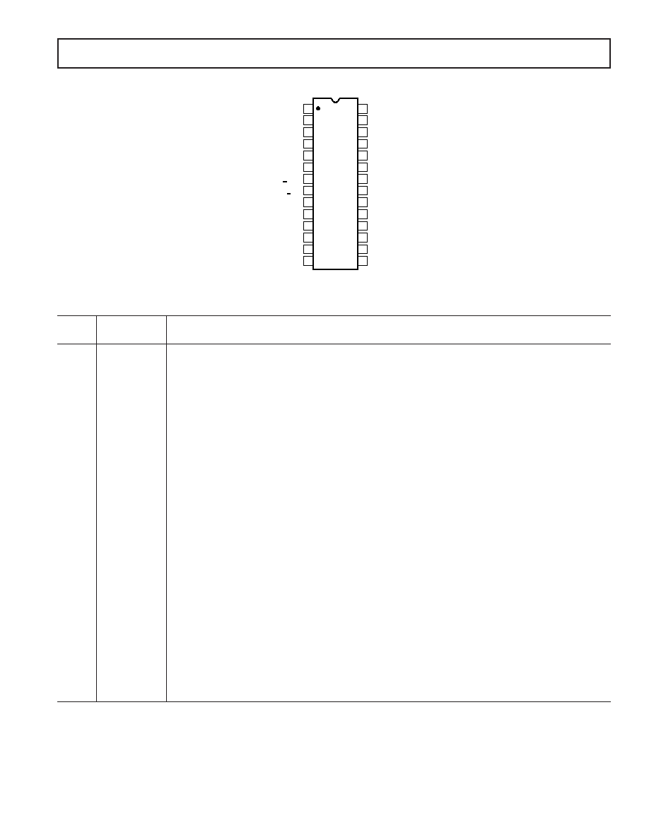
PIN CONFIGURATION
17
16
15
20
19
18
28
27
26
25
24
23
22
21
14
13
12
11
10
9
8
1
2
3
4
7
6
5
TOP VIEW
(Not to Scale)
AD9850
D3
D7 MSB/SERIAL LOAD
D6
D5
D4
D2
D1
LSB D0
RESET
DVDD
DGND
DVDD
W CLK
FQ UD
CLKIN
AGND
IOUTB
IOUT
AVDD
RSET
QOUTB
QOUT
AVDD
VINN
VINP
DACBL (NC)
NC = NO CONNECT
Table I. PIN FUNCTION DESCRIPTIONS
Pin
No.
Mnemonic
Function
4 to 1,
D0 to D7
8-Bit Data Input. This is the 8-bit data port for iteratively loading the 32-bit frequency and the 8-bit phase/
28 to 25
control word. D7 = MSB; D0 = LSB. D7 (Pin 25) also serves as the input pin for the 40-bit serial data-word.
5, 24
DGND
Digital Ground. These are the ground return leads for the digital circuitry.
6, 23
DVDD
Supply Voltage Leads for Digital Circuitry.
7W_CLK
Word Load Clock. This clock is used to load the parallel or serial frequency/phase/control words.
8
FQ_UD
Frequency Update. On the rising edge of this clock, the DDS updates to the frequency (or phase)
loaded in the data input register; it then resets the pointer to Word 0.
9
CLKIN
Reference Clock Input. This may be a continuous CMOS-level pulse train or sine input biased at
1/2 V supply. The rising edge of this clock initiates operation.
10, 19
AGND
Analog Ground. These leads are the ground return for the analog circuitry (DAC and comparator).
11, 18
AVDD
Supply Voltage for the Analog Circuitry (DAC and Comparator).
12
RSET
DAC’s External RSET Connection. This resistor value sets the DAC full-scale output current. For
normal applications (FS IOUT = 10 mA), the value for RSET is 3.9 k
connected to ground. The R
SET/IOUT
relationship is IOUT = 32 (1.248 V/RSET).
13
QOUTB
Output Complement. This is the comparator’s complement output.
14
QOUT
Output True. This is the comparator’s true output.
15
VINN
Inverting Voltage Input. This is the comparator’s negative input.
16
VINP
Noninverting Voltage Input. This is the comparator’s positive input.
17
DACBL (NC)
DAC Baseline. This is the DAC baseline voltage reference; this lead is internally bypassed and should
normally be considered a no connect for optimum performance.
20
IOUTB
Complementary Analog Output of the DAC.
21
IOUT
Analog Current Output of the DAC.
22
RESET
Reset. This is the master reset function; when set high, it clears all registers (except the input register), and
the DAC output goes to cosine 0 after additional clock cycles—see Figure 7.
相关PDF资料 |
PDF描述 |
|---|---|
| VE-B1K-IW-B1 | CONVERTER MOD DC/DC 40V 100W |
| AD9835BRUZ | IC DDS 10BIT 50MHZ 16-TSSOP |
| VE-B1L-IW-B1 | CONVERTER MOD DC/DC 28V 100W |
| AD9859YSVZ | IC DDS DAC 10BIT 400MSPS 48-TQFP |
| VE-B1K-IX-B1 | CONVERTER MOD DC/DC 40V 75W |
相关代理商/技术参数 |
参数描述 |
|---|---|
| AD9850BRSZ | 制造商:Analog Devices 功能描述:IC, DDS, 125MHz, SSOP-28 |
| AD9850BRSZ-REEL | 功能描述:IC DDS SYNTHESIZER CMOS 28-SSOP RoHS:是 类别:集成电路 (IC) >> 接口 - 直接数字合成 (DDS) 系列:- 产品变化通告:Product Discontinuance 27/Oct/2011 标准包装:2,500 系列:- 分辨率(位):10 b 主 fclk:25MHz 调节字宽(位):32 b 电源电压:2.97 V ~ 5.5 V 工作温度:-40°C ~ 85°C 安装类型:表面贴装 封装/外壳:16-TSSOP(0.173",4.40mm 宽) 供应商设备封装:16-TSSOP 包装:带卷 (TR) |
| AD9851 | 制造商:AD 制造商全称:Analog Devices 功能描述:CMOS 180 MHz DDS/DAC Synthesizer |
| AD9851/CGPCB | 制造商:Analog Devices 功能描述:NCO/DDS, CMOS 180MHZ DDS/DAC SYNTHESIZER - Bulk 制造商:Rochester Electronics LLC 功能描述:DDS CLOCK DRIVER - Bulk |
| AD9851/FSPCB | 制造商:Analog Devices 功能描述:Evaluation Board For NCO/DDS, CMOS 180MHZ DDS/DAC Synthesizer 制造商:Analog Devices 功能描述:NCO/DDS, CMOS 180MHZ DDS/DAC SYNTHESIZER - Bulk |
发布紧急采购,3分钟左右您将得到回复。