- 您现在的位置:买卖IC网 > PDF目录10979 > AD9851BRSZ (Analog Devices Inc)IC SYNTHESIZER DDS/DAC 28-SSOP PDF资料下载
参数资料
| 型号: | AD9851BRSZ |
| 厂商: | Analog Devices Inc |
| 文件页数: | 6/24页 |
| 文件大小: | 0K |
| 描述: | IC SYNTHESIZER DDS/DAC 28-SSOP |
| 产品培训模块: | Direct Digital Synthesis Tutorial Series (1 of 7): Introduction Direct Digital Synthesizer Tutorial Series (7 of 7): DDS in Action Direct Digital Synthesis Tutorial Series (3 of 7): Angle to Amplitude Converter Direct Digital Synthesis Tutorial Series (6 of 7): SINC Envelope Correction Direct Digital Synthesis Tutorial Series (4 of 7): Digital-to-Analog Converter Direct Digital Synthesis Tutorial Series (2 of 7): The Accumulator |
| 标准包装: | 1 |
| 分辨率(位): | 10 b |
| 主 fclk: | 180MHz |
| 调节字宽(位): | 32 b |
| 电源电压: | 2.7 V ~ 5.25 V |
| 工作温度: | -40°C ~ 85°C |
| 安装类型: | 表面贴装 |
| 封装/外壳: | 28-SSOP(0.209",5.30mm 宽) |
| 供应商设备封装: | 28-SSOP |
| 包装: | 管件 |
| 产品目录页面: | 552 (CN2011-ZH PDF) |
AD9851
–14–
the factory test mode. Exit from serial mode to parallel mode is
only possible using the RESET command.
The function assignments of the data and control words are shown
in Tables I and III; the detailed timing sequence for updating the
output frequency and/or phase, resetting the device, engaging the
6 REFCLK multiplier, and powering up/down, are shown in
the timing diagrams of Figures 13 through 20. As a programming
example for the following DDS characteristics:
1. Phase set to 11.25°
2. 6 REFCLK multiplier engaged
3. Powered-up mode selected
4. Output = 10 MHz (for 180 MHz system clock)
In parallel mode, user would program the 40-bit control word
(composed of five 8-bit loads) as follows:
W0 = 00001001
W1 = 00001110
W2 = 00111000
W3 = 11100011
W4 = 10001110
If in serial mode, load the 40 bits starting from the LSB location
of W4 in the above array, loading from right to left, and ending
with the MSB of W0.
Table I. 8-Bit Parallel-Load Data/Control Word Functional Assignment
Word
Data[7]
Data[6]
Data[5]
Data[4]
Data[3]
Data[2]
Data[1]
Data[0]
W0
Phase–b4 (MSB)
Phase–b3
Phase–b2
Phase–b1
Phase–b0 (LSB)
Power-Down
Logic 0*
6 REFCLK
Multiplier Enable
W1
Freq–b31 (MSB)
Freq–b30
Freq–b29
Freq–b28
Freq–b27
Freq–b26
Freq–b25
Freq–b24
W2
Freq–b23
Freq–b22
Freq–b21
Freq–b20
Freq–b19
Freq–b18
Freq–b17
Freq–b16
W3
Freq–b15
Freq–b14
Freq–b13
Freq–b12
Freq–b11
Freq–b10
Freq–b9
Freq–b8
W4
Freq–b7
Freq–b6
Freq–b5
Freq–b4
Freq–b3
Freq–b2
Freq–b1
Freq–b0 (LSB)
*This bit is always Logic 0 unless invoking the serial mode (see Figure 17). After serial mode is entered, this data bit must be set back to Logic 0 for proper operation.
W0*
W1
W2
W3
W4
tCD
tDH
tDS
tWL
tWH
tFD
ttttttFH
FH
tttttFL
FL
*OUTPUT UPDATE CAN OCCUR AFTER ANY WORD LOAD
AND IS ASYNCHRONOUS WITH REFERENCE CLOCK
tttttCF
CF
VALID DATA
SYSCLK
DATA
W CLK
FQ UD
AOUT
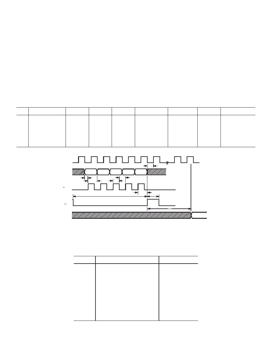
Figure 13. Parallel Load Frequency/Phase UpdateTiming Sequence
Note:To update W0 it is not necessary to load W1 through W4. Simply load W0 and assert FQ_UD.To update W1, reload W0 then W1— users do not have random access to
programming words.
Table II. Timing Specifications
Symbol
Definition
Min
tDS
Data Setup Time
3.5 ns
tDH
Data Hold Time
3.5 ns
tWH
W_CLK High
3.5 ns
tWL
W_CLK Low
3.5 ns
tCD
REFCLK Delay after FQ_UD
3.5 ns*
tFH
FQ_UD High
7.0 ns
tFL
FQ_UD Low
7.0 ns
tFD
FQ_UD Delay after W_CLK
7.0 ns
tCF
Output Latency from FQ_UD
Frequency Change
18 SYSCLK Cycles
Phase Change
13 SYSCLK Cycles
*Specification does not apply when the 6 REFCLK multiplier is engaged.
REV. D
相关PDF资料 |
PDF描述 |
|---|---|
| S9S08DZ96F2MLF | MCU 96K FLASH MASK AUTO 48-LQFP |
| AD9850BRSZ | IC DDS SYNTHESIZER CMOS 28-SSOP |
| VE-B1K-IW-B1 | CONVERTER MOD DC/DC 40V 100W |
| AD9835BRUZ | IC DDS 10BIT 50MHZ 16-TSSOP |
| VE-B1L-IW-B1 | CONVERTER MOD DC/DC 28V 100W |
相关代理商/技术参数 |
参数描述 |
|---|---|
| AD9851BRSZ | 制造商:Analog Devices 功能描述:Direct Digital Synthesizer IC (DDS) |
| AD9851BRSZRL | 功能描述:IC SYNTHESR DDS/DAC 28SSOP TR RoHS:是 类别:集成电路 (IC) >> 接口 - 直接数字合成 (DDS) 系列:- 产品变化通告:Product Discontinuance 27/Oct/2011 标准包装:2,500 系列:- 分辨率(位):10 b 主 fclk:25MHz 调节字宽(位):32 b 电源电压:2.97 V ~ 5.5 V 工作温度:-40°C ~ 85°C 安装类型:表面贴装 封装/外壳:16-TSSOP(0.173",4.40mm 宽) 供应商设备封装:16-TSSOP 包装:带卷 (TR) |
| AD9851CGPCB | 制造商:AD 制造商全称:Analog Devices 功能描述:CMOS 180 MHz DDS/DAC Synthesizer |
| AD9851FSPCB | 制造商:Analog Devices 功能描述:EVALUATION BOARD ((NS)) |
| AD9852 | 制造商:AD 制造商全称:Analog Devices 功能描述:CMOS 300 MHz Complete-DDS |
发布紧急采购,3分钟左右您将得到回复。