- 您现在的位置:买卖IC网 > PDF目录378276 > AD9878-EB (Analog Devices, Inc.) Mixed-Signal Front End for Broadband Applications PDF资料下载
参数资料
| 型号: | AD9878-EB |
| 厂商: | Analog Devices, Inc. |
| 元件分类: | 模拟前端 |
| 英文描述: | Mixed-Signal Front End for Broadband Applications |
| 中文描述: | 混合信号的宽带应用前端 |
| 文件页数: | 18/36页 |
| 文件大小: | 749K |
| 代理商: | AD9878-EB |
第1页第2页第3页第4页第5页第6页第7页第8页第9页第10页第11页第12页第13页第14页第15页第16页第17页当前第18页第19页第20页第21页第22页第23页第24页第25页第26页第27页第28页第29页第30页第31页第32页第33页第34页第35页第36页
AD9878
SERIAL INTERFACE FOR REGISTER CONTROL
The AD9878 serial port is a flexible, synchronous, serial
communications port that allows easy interface to many
industry-standard microcontrollers and microprocessors.
The interface allows read/write access to all registers that
configure the AD9878. Single or multiple byte transfers are
supported. Also, the interface can be programmed to read words
either MSB first or LSB first. The AD9878 serial interface port
I/O can be configured to have one bidirectional I/O (SDIO)
pin, or two unidirectional I/O (SDIO/SDO) pins.
Rev. A | Page 18 of 36
GENERAL OPERATION OF THE SERIAL INTERFACE
There are two phases of a communication cycle with the AD9878.
Phase 1 is the instruction cycle, which is the writing of an in-
struction byte into the AD9878, coincident with the first eight
SCLK rising edges. The instruction byte provides the AD9878
serial port controller with information regarding the data transfer
cycle, which is Phase 2 of the communication cycle.
The Phase 1 instruction byte defines whether the upcoming data
transfer is a read or write, the number of bytes in the data transfer,
and the starting register address for the first byte of the data
transfer. The first eight SCLK rising edges of each communication
cycle are used to write the instruction byte into the AD9878.
The eight remaining SCLK edges are for Phase 2 of the commu-
nication cycle. Phase 2 is the actual data transfer between the
AD9878 and the system controller. Phase 2 of the communication
cycle is a transfer of one to four data bytes, as determined by the
instruction byte. Normally, using one multibyte transfer is the
preferred method. However, single-byte data transfers are useful
to reduce CPU overhead when register access requires only one
byte. Registers change immediately upon writing to the last bit
of each transfer byte.
INSTRUCTION BYTE
The R/W bit of the instruction byte determines whether a read
or a write data transfer occurs after the instruction byte write.
Logic high indicates a read operation; logic low indicates a write
operation. The [N1:N0] bits determine the number of bytes to
be transferred during the data transfer cycle. The bit decodes
are shown in Table 9. The timing diagrams are shown in Figure 19
and Figure 20.
Table 8. Instruction Byte Information
MSB 17
16
15
R/W
N1
N0
14
A4
13
A3
12
A2
11
A1
LSB 10
A0
Table 9. Bit Decodes
N1
0
0
1
1
N0
0
1
0
1
Description
Transfer 1 byte
Transfer 2 bytes
Transfer 3 bytes
Transfer 4 bytes
Bits [A4:A0] determine which register is accessed during the
data transfer portion of the communication cycle. For multi-
byte transfers, this address is the starting byte address. The
remaining register addresses are generated by the AD9878.
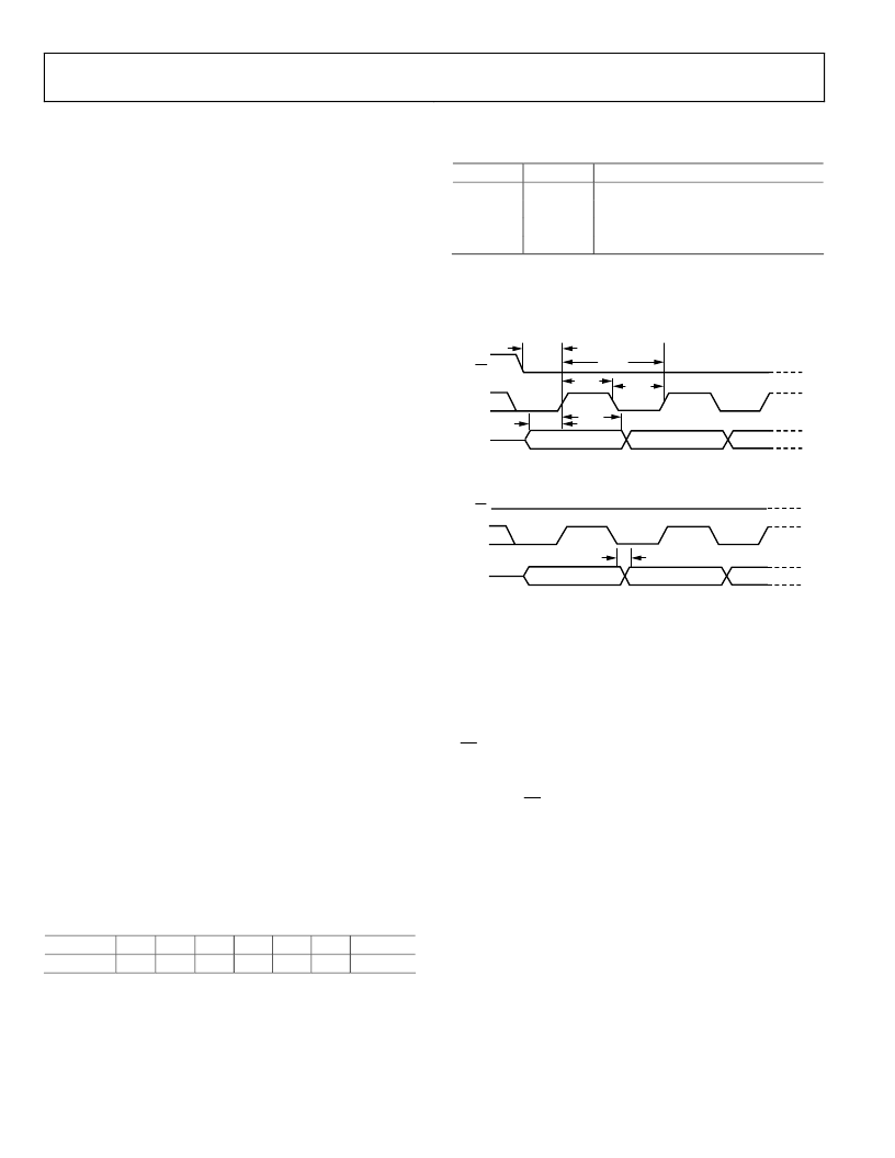
0
SCLK
INSTRUCTION BIT 7
INSTRUCTION BIT 6
t
SCLK
t
DH
t
PWL
t
PWH
t
DS
SDIO
CS
t
DS
Figure 19. Timing Diagram for Register Write
0
SCLK
SDIO
SDO
CS
DATA BIT N
DATA BIT N
t
DV
Figure 20. Timing Diagram for Register Read
SERIAL INTERFACE PORT PIN DESCRIPTIONS
SCLK—Serial Clock. The serial clock pin is used to synchronize
data transfers from the AD9878 and to run the serial port state
machine. The maximum SCLK frequency is 15 MHz. Input data
to the AD9878 is sampled up on the rising edge of SCLK. Output
data changes upon the falling edge of SCLK.
CS—Chip Select. Active low input starts and gates a commu-
nication cycle. It allows multiple devices to share a common
serial port bus. The SDO and SDIO pins go into a high impedance
state when CS is high. Chip select should stay low during the
entire communication cycle.
SDIO—Serial Data I/O. Data is always written into the AD9878
on this pin. However, this pin can be used as a bidirectional
data line. The configuration of this pin is controlled by Bit 7 of
Register 0x00. The default is Logic 0, which configures the SDIO
pin as unidirectional.
SDO—Serial Data Out. Data is read from this pin for protocols
that use separate lines for transmitting and receiving data. In
the case where the AD9878 operates in a single bidirectional
I/O mode, this pin does not output data and is set to a high
impedance state.
相关PDF资料 |
PDF描述 |
|---|---|
| AD9878BST | Mixed-Signal Front End for Broadband Applications |
| AD9878BSTZ | Mixed-Signal Front End for Broadband Applications |
| ADAV801 | Audio Codec for Recordable DVD |
| ADAV801ASTZ | Audio Codec for Recordable DVD |
| ADAV801ASTZ-REEL | Audio Codec for Recordable DVD |
相关代理商/技术参数 |
参数描述 |
|---|---|
| AD9879 | 制造商:AD 制造商全称:Analog Devices 功能描述:Mixed-Signal Front End Set-Top Box, Cable Modem |
| AD9879_05 | 制造商:AD 制造商全称:Analog Devices 功能描述:Mixed-Signal Front End Set-Top Box, Cable Modem |
| AD9879BS | 制造商:Analog Devices 功能描述: |
| AD9879BSZ | 功能描述:IC PROCESSOR FRONT END 100MQFP RoHS:是 类别:集成电路 (IC) >> 数据采集 - 模拟前端 (AFE) 系列:- 产品培训模块:Lead (SnPb) Finish for COTS Obsolescence Mitigation Program 标准包装:2,500 系列:- 位数:- 通道数:2 功率(瓦特):- 电压 - 电源,模拟:3 V ~ 3.6 V 电压 - 电源,数字:3 V ~ 3.6 V 封装/外壳:32-VFQFN 裸露焊盘 供应商设备封装:32-QFN(5x5) 包装:带卷 (TR) |
| AD9879BSZKL1 | 制造商:Rochester Electronics LLC 功能描述: 制造商:Analog Devices 功能描述: |
发布紧急采购,3分钟左右您将得到回复。