- 您现在的位置:买卖IC网 > PDF目录378276 > AD9878BSTZ (ANALOG DEVICES INC) Mixed-Signal Front End for Broadband Applications PDF资料下载
参数资料
| 型号: | AD9878BSTZ |
| 厂商: | ANALOG DEVICES INC |
| 元件分类: | 通信及网络 |
| 英文描述: | Mixed-Signal Front End for Broadband Applications |
| 中文描述: | SPECIALTY TELECOM CIRCUIT, PQFP100 |
| 封装: | LEAD FREE, MS-026BED, LQFP-100 |
| 文件页数: | 26/36页 |
| 文件大小: | 749K |
| 代理商: | AD9878BSTZ |
第1页第2页第3页第4页第5页第6页第7页第8页第9页第10页第11页第12页第13页第14页第15页第16页第17页第18页第19页第20页第21页第22页第23页第24页第25页当前第26页第27页第28页第29页第30页第31页第32页第33页第34页第35页第36页
AD9878
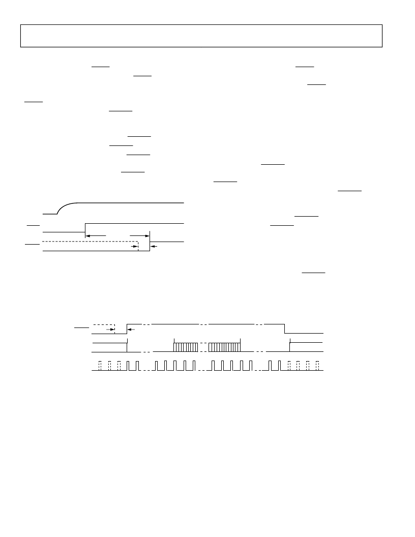
POWER-UP SEQUENCE
Upon initial power-up, the RESET pin should be held low until the
power supply is stable (see Figure 30). Once RESET is deasserted,
the AD9878 can be programmed over the serial port. The on-
chip PLL requires a maximum of 1 ms after the rising edge of
RESET or a change of the multiplier factor (M) to completely
settle. It is recommended that the PWRDN pin is held low during
the reset and PLL settling time. Changes to ADC clock select
(Register 0x08) or System Clock Divider N (Register 0x01) should
be programmed before the rising edge of PWRDN. Once the PLL
is frequency locked and after the PWRDN pin is brought high,
transmit data can be sent reliably. If the PWRDN pin cannot be
held low throughout the reset and PLL settling time period,
the power-down digital Tx bit, or the PWRDN pin, should be
pulsed after the PLL has settled. This ensures correct transmit
filter initialization.
Rev. A | Page 26 of 36
0
V
S
1ms MIN.
5MCLK MIN.
RESET
PWRDN
Figure 30. Power-Up Sequence for Tx Data Path
RESET
To initiate a hardware reset, the RESET pin should be held low
for at least 100 ns. All internally generated clocks, except REFCLK,
stop during reset. The rising edge of RESET resets the PLL clock
multiplier and reinitializes the programmable registers to their
default values. The same sequence as described in the Power-Up
Sequence section should be followed after a reset or change in M.
A software reset (writing 1 into Bit 5 of Register 0x00) is func-
tionally equivalent to a hardware reset, but does not force
Register 0x00 to its default value.
TRANSMIT POWER-DOWN
A low level on the PWRDN pin stops all clocks linked to the
digital transmit data path and resets the CIC filter. Deasserting
PWRDN reactivates all clocks. The CIC filter is held in a reset
state for 80 MCLK cycles after the rising edge of PWRDN to
allow for flushing of the half-band filters with new input data.
Transmit data bursts should be padded with at least 20 symbols
of null data directly before the PWRDN pin is deasserted.
Immediately after the PWRDN pin is deasserted, the transmit
burst should start with a minimum of 20 null data symbols (see
Figure 31). This avoids unintended DAC output samples caused
by the transmit path latency and filter settling time.
Software power-down digital Tx (Bit 5 in Register 0x02) is func-
tionally equivalent to the hardware PWRDN pin and takes effect
immediately after the last register bit is written over the serial port.
PWRDN
TxIQ
TxSYNC
20 NULL SYMBOLS
DATA SYMBOLS
20 NULL SYMBOLS
0
0
0
0
0
0
0
0
5MCLK MIN.
0
Figure 31. Timing Sequence to Flush Tx Data Path
相关PDF资料 |
PDF描述 |
|---|---|
| ADAV801 | Audio Codec for Recordable DVD |
| ADAV801ASTZ | Audio Codec for Recordable DVD |
| ADAV801ASTZ-REEL | Audio Codec for Recordable DVD |
| ADC0800PCD | ADC0800 8-Bit A/D Converter |
| ADC0800PD | ADC0800 8-Bit A/D Converter |
相关代理商/技术参数 |
参数描述 |
|---|---|
| AD9878-EB | 制造商:Analog Devices 功能描述:EVAL KIT FOR MIXED-SGNL FRONT END FOR BROADBAND APPLICATIONS - Bulk |
| AD9879 | 制造商:AD 制造商全称:Analog Devices 功能描述:Mixed-Signal Front End Set-Top Box, Cable Modem |
| AD9879_05 | 制造商:AD 制造商全称:Analog Devices 功能描述:Mixed-Signal Front End Set-Top Box, Cable Modem |
| AD9879BS | 制造商:Analog Devices 功能描述: |
| AD9879BSZ | 功能描述:IC PROCESSOR FRONT END 100MQFP RoHS:是 类别:集成电路 (IC) >> 数据采集 - 模拟前端 (AFE) 系列:- 产品培训模块:Lead (SnPb) Finish for COTS Obsolescence Mitigation Program 标准包装:2,500 系列:- 位数:- 通道数:2 功率(瓦特):- 电压 - 电源,模拟:3 V ~ 3.6 V 电压 - 电源,数字:3 V ~ 3.6 V 封装/外壳:32-VFQFN 裸露焊盘 供应商设备封装:32-QFN(5x5) 包装:带卷 (TR) |
发布紧急采购,3分钟左右您将得到回复。