- 您现在的位置:买卖IC网 > PDF目录11670 > AD9943KCPZ (Analog Devices Inc)IC CCD SIGNAL PROCESSOR 32-LFCSP PDF资料下载
参数资料
| 型号: | AD9943KCPZ |
| 厂商: | Analog Devices Inc |
| 文件页数: | 6/20页 |
| 文件大小: | 0K |
| 描述: | IC CCD SIGNAL PROCESSOR 32-LFCSP |
| 标准包装: | 1 |
| 类型: | CCD 信号处理器,10 位 |
| 输入类型: | 逻辑 |
| 输出类型: | 逻辑 |
| 接口: | 3 线串口 |
| 安装类型: | 表面贴装 |
| 封装/外壳: | 32-VFQFN 裸露焊盘,CSP |
| 供应商设备封装: | 32-LFCSP-VQ(5x5) |
| 包装: | 托盘 |
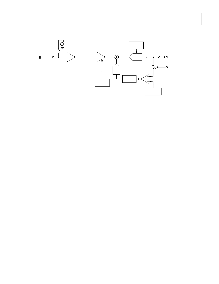
AD9943/AD9944
Data Sheet
CIRCUIT DESCRIPTION AND OPERATION
Figure 12. CCD Mode Block Diagram
Figure 12. Each processing step is essential for achieving a high
quality image from the raw CCD pixel data.
DC RESTORE
To reduce the large dc offset of the CCD output signal, a dc
restore circuit is used with an external 0.1 F series coupling
capacitor. This restores the dc level of the CCD signal to
approximately 1.5 V, which is compatible with the 3 V single
CORRELATED DOUBLE SAMPLER
The CDS circuit samples each CCD pixel twice to extract video
information and reject low frequency noise. The timing shown
in Figure 14 illustrates how the two CDS clocks, SHP and SHD,
are used, respectively, to sample the reference level and data
level of the CCD signal. The CCD signal is sampled on the
rising edges of SHP and SHD. Placement of these two clock
signals is critical for achieving the best performance from the
CCD. An internal SHP/SHD delay (tID) of 3 ns is caused by
internal propagation delays.
OPTICAL BLACK CLAMP
The optical black clamp loop is used to remove residual offsets
in the signal chain and to track low frequency variations in the
CCD’s black level. During the optical black (shielded) pixel
interval on each line, the ADC output is compared with the
fixed black level reference selected by the user in the clamp level
register. The resulting error signal is filtered to reduce noise,
and the correction value is applied to the ADC input through a
D/A converter. Normally, the optical black clamp loop is turned
on once per horizontal line, but this loop can be updated more
slowly to suit a particular application. If external digital
clamping is used during the post processing, the optical black
Bit D3 in the operation register. Refer to Table 8 and Figure 10
and Figure 11.
When the loop is disabled, the clamp level register may still be
used to provide programmable offset adjustment. Horizontal
timing is shown in Figure 15. The CLPOB pulse should be
placed during the CCD’s optical black pixels. It is recommended
that the CLPOB pulse be used during valid CCD dark pixels.
The CLPOB pulse should be a minimum of 20 pixels wide to
minimize clamp noise. Shorter pulse widths may be used, but
clamp noise may increase and the loop’s ability to track low
frequency variations in the black level is reduced.
6dB TO 40dB
CCDIN
DIGITAL
FILTERING
CLPOB
DC RESTORE
OPTICAL BLACK
CLAMP
DOUT
10-/12-BIT
ADC
VGA
8-BIT
DAC
CLAMP LEVEL
REGISTER
8
VGA GAIN
REGISTER
10
CDS
INTERNAL
VREF
2V FULL SCALE
10/12
0.1
F
02905-B-013
Rev. C | Page 14 of 20
相关PDF资料 |
PDF描述 |
|---|---|
| AD8497CRMZ | IC THERMOCOUPLE A W/COMP 8MSOP |
| AD8496CRMZ | THERMOCOUPLE AMPLIFIER I |
| VE-J3N-IY-F2 | CONVERTER MOD DC/DC 18.5V 50W |
| AD8495CRMZ | IC THERMOCOUPLE A W/COMP 8MSOP |
| VI-B32-CU-S | CONVERTER MOD DC/DC 15V 200W |
相关代理商/技术参数 |
参数描述 |
|---|---|
| AD9943KCPZ1 | 制造商:AD 制造商全称:Analog Devices 功能描述:Complete 10-Bit and 12-Bit, 25 MHz CCD Signal Processors |
| AD9943KCPZRL | 功能描述:IC CCD SIGNAL PROCESS 32LFCSP TR RoHS:是 类别:集成电路 (IC) >> 接口 - 传感器和探测器接口 系列:- 其它有关文件:Automotive Product Guide 产品培训模块:Lead (SnPb) Finish for COTS Obsolescence Mitigation Program 标准包装:74 系列:- 类型:触控式传感器 输入类型:数字 输出类型:数字 接口:JTAG,串行 电流 - 电源:100µA 安装类型:表面贴装 封装/外壳:20-TSSOP(0.173",4.40mm 宽) 供应商设备封装:20-TSSOP 包装:管件 |
| AD9943KCPZRL1 | 制造商:AD 制造商全称:Analog Devices 功能描述:Complete 10-Bit and 12-Bit, 25 MHz CCD Signal Processors |
| AD9943-WAFER | 功能描述:IC CCD SIGNAL PROCESSOR 制造商:analog devices inc. 系列:- 包装:散装 零件状态:上次购买时间 类型:CCD 信号处理器,10 位 输入类型:逻辑 输出类型:逻辑 接口:3 线串口 电流 - 电源:- 工作温度:-20°C ~ 85°C 安装类型:表面贴装 封装/外壳:模具 供应商器件封装:模具 标准包装:1 |
| AD9944 | 制造商:AD 制造商全称:Analog Devices 功能描述:Complete 10-Bit and 12-Bit, 25 MHz CCD Signal Processors |
发布紧急采购,3分钟左右您将得到回复。