- 您现在的位置:买卖IC网 > PDF目录3935 > MPC8544EAVTALFA (Freescale Semiconductor)IC MPU POWERQUICC III 783-FCBGA PDF资料下载
参数资料
| 型号: | MPC8544EAVTALFA |
| 厂商: | Freescale Semiconductor |
| 文件页数: | 12/117页 |
| 文件大小: | 0K |
| 描述: | IC MPU POWERQUICC III 783-FCBGA |
| 标准包装: | 36 |
| 系列: | MPC85xx |
| 处理器类型: | 32-位 MPC85xx PowerQUICC III |
| 速度: | 667MHz |
| 电压: | 0.95 V ~ 1.05 V |
| 安装类型: | 表面贴装 |
| 封装/外壳: | 783-BBGA,FCBGA |
| 供应商设备封装: | 783-FCPBGA(29x29) |
| 包装: | 托盘 |
第1页第2页第3页第4页第5页第6页第7页第8页第9页第10页第11页当前第12页第13页第14页第15页第16页第17页第18页第19页第20页第21页第22页第23页第24页第25页第26页第27页第28页第29页第30页第31页第32页第33页第34页第35页第36页第37页第38页第39页第40页第41页第42页第43页第44页第45页第46页第47页第48页第49页第50页第51页第52页第53页第54页第55页第56页第57页第58页第59页第60页第61页第62页第63页第64页第65页第66页第67页第68页第69页第70页第71页第72页第73页第74页第75页第76页第77页第78页第79页第80页第81页第82页第83页第84页第85页第86页第87页第88页第89页第90页第91页第92页第93页第94页第95页第96页第97页第98页第99页第100页第101页第102页第103页第104页第105页第106页第107页第108页第109页第110页第111页第112页第113页第114页第115页第116页第117页
MPC8544E PowerQUICC III Integrated Processor Hardware Specifications, Rev. 6
Freescale Semiconductor
109
System Design Information
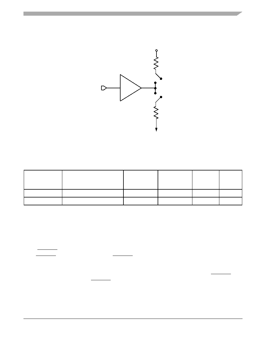
and RP is trimmed until the voltage at the pad equals OVDD/2. RP then becomes the resistance of the
pull-up devices. RP and RN are designed to be close to each other in value. Then, Z0 =(RP +RN) ÷ 2.
Figure 67. Driver Impedance Measurement
Table 73 summarizes the signal impedance targets. The driver impedances are targeted at minimum VDD,
nominal OVDD, 90° C.
21.8
Configuration Pin Muxing
The MPC8544E provides the user with power-on configuration options which can be set through the use
of external pull-up or pull-down resistors of 4.7 k
Ωon certain output pins (see customer visible
configuration pins). These pins are generally used as output only pins in normal operation.
While HRESET is asserted however, these pins are treated as inputs. The value presented on these pins
while HRESET is asserted, is latched when HRESET deasserts, at which time the input receiver is disabled
and the I/O circuit takes on its normal function. Most of these sampled configuration pins are equipped
with an on-chip gated resistor of approximately 20 k
Ω. This value should permit the 4.7-kΩ resistor to pull
the configuration pin to a valid logic low level. The pull-up resistor is enabled only during HRESET (and
for platform /system clocks after HRESET deassertion to ensure capture of the reset value). When the input
receiver is disabled the pull-up is also, thus allowing functional operation of the pin as an output with
minimal signal quality or delay disruption. The default value for all configuration bits treated this way has
Table 73. Impedance Characteristics
Impedance
Local Bus, Ethernet, DUART,
Control, Configuration, Power
Management
PCI
DDR DRAM
Symbol
Unit
RN
43 Target
25 Target
20 Target
Z0
W
RP
43 Target
25 Target
20 Target
Z0
W
Note: Nominal supply voltages. See Table 1.
OVDD
OGND
RP
RN
Pad
Data
SW1
SW2
相关PDF资料 |
PDF描述 |
|---|---|
| SLW5S-5C7LF | CONN ZIF CIC 5POS DIP 1MM VERT |
| XF2L-0735-1A | CONNECTOR FPC 7POS 0.5MM SMD |
| XF2L-0725-1A | CONN FPC 7POS 0.5MM PITCH SMD |
| CAT24C32HU4I-GT3 | IC EEPROM 32KBIT 400KHZ 8UDFN |
| 346-020-522-802 | CARDEDGE 20POS DUAL .125 GREEN |
相关代理商/技术参数 |
参数描述 |
|---|---|
| ADA4084-2ACPZ-RL | 功能描述:IC OPAMP GP RRIO 10MHZ DL 8LFCSP RoHS:是 类别:集成电路 (IC) >> Linear - Amplifiers - Instrumentation 系列:- 标准包装:100 系列:- 放大器类型:通用 电路数:1 输出类型:- 转换速率:0.2 V/µs 增益带宽积:- -3db带宽:- 电流 - 输入偏压:100pA 电压 - 输入偏移:30µV 电流 - 电源:380µA 电流 - 输出 / 通道:- 电压 - 电源,单路/双路(±):±2 V ~ 18 V 工作温度:0°C ~ 70°C 安装类型:表面贴装 封装/外壳:8-SOIC(0.154",3.90mm 宽) 供应商设备封装:8-SO 包装:管件 |
| ADA4084-2ARMZ | 功能描述:IC OPAMP GP RRIO 10MHZ DL 8MSOP RoHS:是 类别:集成电路 (IC) >> Linear - Amplifiers - Instrumentation 系列:- 标准包装:2,500 系列:- 放大器类型:通用 电路数:4 输出类型:- 转换速率:0.6 V/µs 增益带宽积:1MHz -3db带宽:- 电流 - 输入偏压:45nA 电压 - 输入偏移:2000µV 电流 - 电源:1.4mA 电流 - 输出 / 通道:40mA 电压 - 电源,单路/双路(±):3 V ~ 32 V,±1.5 V ~ 16 V 工作温度:0°C ~ 70°C 安装类型:表面贴装 封装/外壳:14-TSSOP(0.173",4.40mm 宽) 供应商设备封装:14-TSSOP 包装:带卷 (TR) 其它名称:LM324ADTBR2G-NDLM324ADTBR2GOSTR |
| ADA4084-2ARMZ | 制造商:Analog Devices 功能描述:IC OP-AMP 13.9MHZ 4.6V/ 130 MSO |
| ADA4084-2ARMZ_PROMO | 制造商:Analog Devices 功能描述:IC OP AMP 30V MSOP-8 |
| ADA4084-2ARMZ-R7 | 功能描述:IC OPAMP GP RRIO 10MHZ DL 8MSOP RoHS:是 类别:集成电路 (IC) >> Linear - Amplifiers - Instrumentation 系列:- 标准包装:1 系列:- 放大器类型:通用 电路数:4 输出类型:满摆幅 转换速率:0.028 V/µs 增益带宽积:105kHz -3db带宽:- 电流 - 输入偏压:3nA 电压 - 输入偏移:100µV 电流 - 电源:3.3µA 电流 - 输出 / 通道:12mA 电压 - 电源,单路/双路(±):2.7 V ~ 12 V,±1.35 V ~ 6 V 工作温度:-40°C ~ 85°C 安装类型:表面贴装 封装/外壳:14-TSSOP(0.173",4.40mm 宽) 供应商设备封装:14-TSSOP 包装:剪切带 (CT) 其它名称:OP481GRUZ-REELCT |
发布紧急采购,3分钟左右您将得到回复。