- 您现在的位置:买卖IC网 > PDF目录3935 > MPC8544EAVTALFA (Freescale Semiconductor)IC MPU POWERQUICC III 783-FCBGA PDF资料下载
参数资料
| 型号: | MPC8544EAVTALFA |
| 厂商: | Freescale Semiconductor |
| 文件页数: | 82/117页 |
| 文件大小: | 0K |
| 描述: | IC MPU POWERQUICC III 783-FCBGA |
| 标准包装: | 36 |
| 系列: | MPC85xx |
| 处理器类型: | 32-位 MPC85xx PowerQUICC III |
| 速度: | 667MHz |
| 电压: | 0.95 V ~ 1.05 V |
| 安装类型: | 表面贴装 |
| 封装/外壳: | 783-BBGA,FCBGA |
| 供应商设备封装: | 783-FCPBGA(29x29) |
| 包装: | 托盘 |
第1页第2页第3页第4页第5页第6页第7页第8页第9页第10页第11页第12页第13页第14页第15页第16页第17页第18页第19页第20页第21页第22页第23页第24页第25页第26页第27页第28页第29页第30页第31页第32页第33页第34页第35页第36页第37页第38页第39页第40页第41页第42页第43页第44页第45页第46页第47页第48页第49页第50页第51页第52页第53页第54页第55页第56页第57页第58页第59页第60页第61页第62页第63页第64页第65页第66页第67页第68页第69页第70页第71页第72页第73页第74页第75页第76页第77页第78页第79页第80页第81页当前第82页第83页第84页第85页第86页第87页第88页第89页第90页第91页第92页第93页第94页第95页第96页第97页第98页第99页第100页第101页第102页第103页第104页第105页第106页第107页第108页第109页第110页第111页第112页第113页第114页第115页第116页第117页
MPC8544E PowerQUICC III Integrated Processor Hardware Specifications, Rev. 6
Freescale Semiconductor
67
High-Speed Serial Interfaces (HSSI)
— For external DC-coupled connection, as described in Section 16.2.1, “SerDes Reference
Clock Receiver Characteristics,” the maximum average current requirements sets the
requirement for average voltage (common mode voltage) to be between 100 and 400 mV.
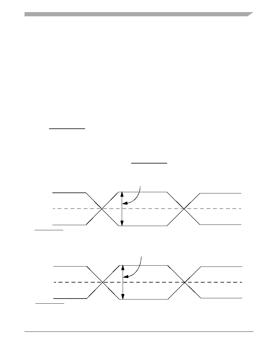
Figure 46 shows the SerDes reference clock input requirement for DC-coupled connection
scheme.
— For external AC-coupled connection, there is no common mode voltage requirement for the
clock driver. Since the external AC-coupling capacitor blocks the DC level, the clock driver and
the SerDes reference clock receiver operate in different command mode voltages. The SerDes
reference clock receiver in this connection scheme has its common mode voltage set to
SGND_SRDSn. Each signal wire of the differential inputs is allowed to swing below and above
the command mode voltage (SGND_SRDSn). Figure 47 shows the SerDes reference clock
input requirement for AC-coupled connection scheme.
Single-ended Mode
— The reference clock can also be single-ended. The SDn_REF_CLK input amplitude
(single-ended swing) must be between 400 and 800 mV peak-peak (from Vmin to Vmax) with
SDn_REF_CLK either left unconnected or tied to ground.
—The SDn_REF_CLK input average voltage must be between 200 and 400 mV. Figure 48 shows
the SerDes reference clock input requirement for single-ended signaling mode.
— To meet the input amplitude requirement, the reference clock inputs might need to be DC or
AC-coupled externally. For the best noise performance, the reference of the clock could be DC
or AC-coupled into the unused phase (SDn_REF_CLK) through the same source impedance as
the clock input (SDn_REF_CLK) in use.
Figure 46. Differential Reference Clock Input DC Requirements (External DC-Coupled)
Figure 47. Differential Reference Clock Input DC Requirements (External AC-Coupled)
SDn_REF_CLK
Vmax < 800 mV
Vmin > 0 V
100 mV < Vcm < 400 mV
200 mV < Input Amplitude or Differential Peak < 800 mV
SDn_REF_CLK
Vcm
200 mV < Input Amplitude or Differential Peak < 800 mV
Vmax < Vcm + 400 mV
Vmin > Vcm - 400 mV
相关PDF资料 |
PDF描述 |
|---|---|
| SLW5S-5C7LF | CONN ZIF CIC 5POS DIP 1MM VERT |
| XF2L-0735-1A | CONNECTOR FPC 7POS 0.5MM SMD |
| XF2L-0725-1A | CONN FPC 7POS 0.5MM PITCH SMD |
| CAT24C32HU4I-GT3 | IC EEPROM 32KBIT 400KHZ 8UDFN |
| 346-020-522-802 | CARDEDGE 20POS DUAL .125 GREEN |
相关代理商/技术参数 |
参数描述 |
|---|---|
| MPC8544EAVTANG | 功能描述:微处理器 - MPU PQ3 8544E Netwrk Comm Indstrl Cntrl RoHS:否 制造商:Atmel 处理器系列:SAMA5D31 核心:ARM Cortex A5 数据总线宽度:32 bit 最大时钟频率:536 MHz 程序存储器大小:32 KB 数据 RAM 大小:128 KB 接口类型:CAN, Ethernet, LIN, SPI,TWI, UART, USB 工作电源电压:1.8 V to 3.3 V 最大工作温度:+ 85 C 安装风格:SMD/SMT 封装 / 箱体:FBGA-324 |
| MPC8544EAVTANGA | 功能描述:数字信号处理器和控制器 - DSP, DSC PQ38K 8544E RoHS:否 制造商:Microchip Technology 核心:dsPIC 数据总线宽度:16 bit 程序存储器大小:16 KB 数据 RAM 大小:2 KB 最大时钟频率:40 MHz 可编程输入/输出端数量:35 定时器数量:3 设备每秒兆指令数:50 MIPs 工作电源电压:3.3 V 最大工作温度:+ 85 C 封装 / 箱体:TQFP-44 安装风格:SMD/SMT |
| MPC8544EAVTAQG | 功能描述:微处理器 - MPU PQ3 8544E Netwrk Comm Indstrl Cntrl RoHS:否 制造商:Atmel 处理器系列:SAMA5D31 核心:ARM Cortex A5 数据总线宽度:32 bit 最大时钟频率:536 MHz 程序存储器大小:32 KB 数据 RAM 大小:128 KB 接口类型:CAN, Ethernet, LIN, SPI,TWI, UART, USB 工作电源电压:1.8 V to 3.3 V 最大工作温度:+ 85 C 安装风格:SMD/SMT 封装 / 箱体:FBGA-324 |
| MPC8544EAVTAQGA | 功能描述:数字信号处理器和控制器 - DSP, DSC PQ38K 8544E RoHS:否 制造商:Microchip Technology 核心:dsPIC 数据总线宽度:16 bit 程序存储器大小:16 KB 数据 RAM 大小:2 KB 最大时钟频率:40 MHz 可编程输入/输出端数量:35 定时器数量:3 设备每秒兆指令数:50 MIPs 工作电源电压:3.3 V 最大工作温度:+ 85 C 封装 / 箱体:TQFP-44 安装风格:SMD/SMT |
| MPC8544EAVTARJ | 功能描述:微处理器 - MPU PQ3 8544E Netwrk Comm Indstrl Cntrl RoHS:否 制造商:Atmel 处理器系列:SAMA5D31 核心:ARM Cortex A5 数据总线宽度:32 bit 最大时钟频率:536 MHz 程序存储器大小:32 KB 数据 RAM 大小:128 KB 接口类型:CAN, Ethernet, LIN, SPI,TWI, UART, USB 工作电源电压:1.8 V to 3.3 V 最大工作温度:+ 85 C 安装风格:SMD/SMT 封装 / 箱体:FBGA-324 |
发布紧急采购,3分钟左右您将得到回复。