- 您现在的位置:买卖IC网 > PDF目录6037 > ADA4084-2ARMZ (Analog Devices Inc)IC OPAMP GP RRIO 10MHZ DL 8MSOP PDF资料下载
参数资料
| 型号: | ADA4084-2ARMZ |
| 厂商: | Analog Devices Inc |
| 文件页数: | 16/29页 |
| 文件大小: | 0K |
| 描述: | IC OPAMP GP RRIO 10MHZ DL 8MSOP |
| 标准包装: | 50 |
| 放大器类型: | 通用 |
| 电路数: | 2 |
| 输出类型: | 满摆幅 |
| 转换速率: | 4.6 V/µs |
| 增益带宽积: | 15.9MHz |
| -3db带宽: | 13.9MHz |
| 电流 - 输入偏压: | 140nA |
| 电压 - 输入偏移: | 130µV |
| 电流 - 电源: | 625µA |
| 电流 - 输出 / 通道: | 30mA |
| 电压 - 电源,单路/双路(±): | 4 V ~ 36 V,±2 V ~ 18 V |
| 工作温度: | -40°C ~ 125°C |
| 安装类型: | 表面贴装 |
| 封装/外壳: | 8-TSSOP,8-MSOP(0.118",3.00mm 宽) |
| 供应商设备封装: | 8-MSOP |
| 包装: | 管件 |
第1页第2页第3页第4页第5页第6页第7页第8页第9页第10页第11页第12页第13页第14页第15页当前第16页第17页第18页第19页第20页第21页第22页第23页第24页第25页第26页第27页第28页第29页
ADA4084-2
Data Sheet
Rev. C | Page 22 of 28
APPLICATIONS INFORMATION
FUNCTIONAL DESCRIPTION
The ADA4084-2 is a precision single-supply, rail-to-rail operational
amplifier. Intended for portable instrumentation, the ADA4084-2
combines the attributes of precision, wide bandwidth, and low noise
to make it an ideal choice in single-supply applications that require
both ac and precision dc performance. Other low supply voltage
applications for which the ADA4084-2 is well suited are active filters,
audio microphone preamplifiers, power supply control, and tele-
communications. To combine all of these attributes with rail-to-rail
input/output operation, novel circuit design techniques are used.
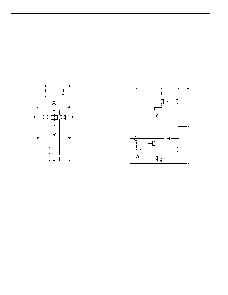
D2
D101
D100
D5
D4
D1
Q1
Q4
Q3
Q2
08237-
073
R4
R1
R2
R3
Figure 78. ADA4084-2 Equivalent Input Circuit
For example, Figure 78 illustrates a simplified equivalent circuit for
the input stage of the ADA4084-2. It comprises a PNP differential
pair, Q1 and Q2, and an NPN differential pair, Q3 and Q4,
operating concurrently. Diode D100 and Diode D101 serve to
clamp the applied differential input voltage to the ADA4084-2,
thereby protecting the input transistors against Zener breakdown
of the emitter-base junctions. Input stage voltage gains are kept
low for input rail-to-rail operation. The two pairs of differential
output voltages are connected to the second stage of the ADA4084-2,
which is a modified compound folded cascade gain stage. It is also
in the second gain stage, where the two pairs of differential output
voltages are combined into a single-ended output signal voltage
used to drive the output stage.
A key issue in the input stage is the behavior of the input bias
currents over the input common-mode voltage range. Input bias
currents in the ADA4084-2 are the arithmetic sum of the base
currents in Q1 and Q4 and in Q2 and Q3. As a result of this design
approach, the input bias currents in the ADA4084-2 not only
exhibit different amplitudes; they also exhibit different polarities.
This effect is best illustrated by Figure 9, Figure 10, Figure 34,
that the effective source impedances connected to the ADA4084-2
inputs be balanced for optimum dc and ac performance.
To achieve rail-to-rail output, the ADA4084-2 output stage
design employs a unique topology for both sourcing and sinking
current. This circuit topology is illustrated in Figure 79. The
output stage is voltage-driven from the second gain stage. The
signal path through the output stage is inverting; that is, for
positive input signals, Q13 provides the base current drive to Q19
so that it conducts (sinks) current. For negative input signals, the
signal path via Q18 → mirror → Q24 provides the base current
drive for Q23 to conduct (source) current. Both transistors
provide output current until they are forced into saturation.
Q24
Q21
D20
Q13
Q18
Q19
Q23
VEE
VOUT
VCC
VBIAS
MIRROR
08237-
074
R5
R6
R7 C2
C1
Figure 79. ADA4084-2 Equivalent Output Circuit
Thus, the saturation voltage of the output transistors sets the
limit on the ADA4084-2 maximum output voltage swing. Output
short-circuit current limiting is determined by the maximum
signal current into the base of Q13 from the second gain stage.
The output stage also exhibits voltage gain. This is accomplished
by the use of common-emitter amplifiers, and, as a result, the
voltage gain of the output stage (thus, the open-loop gain of the
device) exhibits a dependence on the total load resistance at the
output of the ADA4084-2.
相关PDF资料 |
PDF描述 |
|---|---|
| M83-LML3M1N60-0000-000 | CONN HDR 2MM R/A W/SCREW 60POS |
| LT6600IS8-10#PBF | IC AMP DIFF LP FLTR 10MHZ 8-SOIC |
| LT1368CS8#PBF | IC OP-AMP R-R IN/OUT DUAL 8-SOIC |
| M80-5S22605MQ | CONN HDR 2MM R/A W/SCREW 26POS |
| 929665-05-36-I | CONN HEADER .100 DUAL STR 72POS |
相关代理商/技术参数 |
参数描述 |
|---|---|
| ADA4084-2ARMZ | 制造商:Analog Devices 功能描述:IC OP-AMP 13.9MHZ 4.6V/ 130 MSO |
| ADA4084-2ARMZ_PROMO | 制造商:Analog Devices 功能描述:IC OP AMP 30V MSOP-8 |
| ADA4084-2ARMZ-R7 | 功能描述:IC OPAMP GP RRIO 10MHZ DL 8MSOP RoHS:是 类别:集成电路 (IC) >> Linear - Amplifiers - Instrumentation 系列:- 标准包装:1 系列:- 放大器类型:通用 电路数:4 输出类型:满摆幅 转换速率:0.028 V/µs 增益带宽积:105kHz -3db带宽:- 电流 - 输入偏压:3nA 电压 - 输入偏移:100µV 电流 - 电源:3.3µA 电流 - 输出 / 通道:12mA 电压 - 电源,单路/双路(±):2.7 V ~ 12 V,±1.35 V ~ 6 V 工作温度:-40°C ~ 85°C 安装类型:表面贴装 封装/外壳:14-TSSOP(0.173",4.40mm 宽) 供应商设备封装:14-TSSOP 包装:剪切带 (CT) 其它名称:OP481GRUZ-REELCT |
| ADA4084-2ARMZ-RL | 功能描述:IC OPAMP GP RRIO 10MHZ DL 8MSOP RoHS:是 类别:集成电路 (IC) >> Linear - Amplifiers - Instrumentation 系列:- 标准包装:1 系列:- 放大器类型:通用 电路数:4 输出类型:满摆幅 转换速率:0.028 V/µs 增益带宽积:105kHz -3db带宽:- 电流 - 输入偏压:3nA 电压 - 输入偏移:100µV 电流 - 电源:3.3µA 电流 - 输出 / 通道:12mA 电压 - 电源,单路/双路(±):2.7 V ~ 12 V,±1.35 V ~ 6 V 工作温度:-40°C ~ 85°C 安装类型:表面贴装 封装/外壳:14-TSSOP(0.173",4.40mm 宽) 供应商设备封装:14-TSSOP 包装:剪切带 (CT) 其它名称:OP481GRUZ-REELCT |
| ADA4084-2ARZ | 功能描述:IC OPAMP GP RRIO 10MHZ DL 8SOIC RoHS:是 类别:集成电路 (IC) >> Linear - Amplifiers - Instrumentation 系列:- 标准包装:2,500 系列:- 放大器类型:通用 电路数:4 输出类型:- 转换速率:0.6 V/µs 增益带宽积:1MHz -3db带宽:- 电流 - 输入偏压:45nA 电压 - 输入偏移:2000µV 电流 - 电源:1.4mA 电流 - 输出 / 通道:40mA 电压 - 电源,单路/双路(±):3 V ~ 32 V,±1.5 V ~ 16 V 工作温度:0°C ~ 70°C 安装类型:表面贴装 封装/外壳:14-TSSOP(0.173",4.40mm 宽) 供应商设备封装:14-TSSOP 包装:带卷 (TR) 其它名称:LM324ADTBR2G-NDLM324ADTBR2GOSTR |
发布紧急采购,3分钟左右您将得到回复。