参数资料
| 型号: | ADA4084-2ARZ |
| 厂商: | Analog Devices Inc |
| 文件页数: | 18/29页 |
| 文件大小: | 0K |
| 描述: | IC OPAMP GP RRIO 10MHZ DL 8SOIC |
| 标准包装: | 98 |
| 放大器类型: | 通用 |
| 电路数: | 2 |
| 输出类型: | 满摆幅 |
| 转换速率: | 4.6 V/µs |
| 增益带宽积: | 15.9MHz |
| -3db带宽: | 13.9MHz |
| 电流 - 输入偏压: | 140nA |
| 电压 - 输入偏移: | 100µV |
| 电流 - 电源: | 625µA |
| 电流 - 输出 / 通道: | 30mA |
| 电压 - 电源,单路/双路(±): | 4 V ~ 36 V,±2 V ~ 18 V |
| 工作温度: | -40°C ~ 125°C |
| 安装类型: | 表面贴装 |
| 封装/外壳: | 8-SOIC(0.154",3.90mm 宽) |
| 供应商设备封装: | 8-SO |
| 包装: | 管件 |
第1页第2页第3页第4页第5页第6页第7页第8页第9页第10页第11页第12页第13页第14页第15页第16页第17页当前第18页第19页第20页第21页第22页第23页第24页第25页第26页第27页第28页第29页
ADA4084-2
Data Sheet
Rev. C | Page 24 of 28
DESIGNING LOW NOISE CIRCUITS IN SINGLE-
SUPPLY APPLICATIONS
In single-supply applications, devices like the ADA4084-2 extend
the dynamic range of the application through the use of rail-to-rail
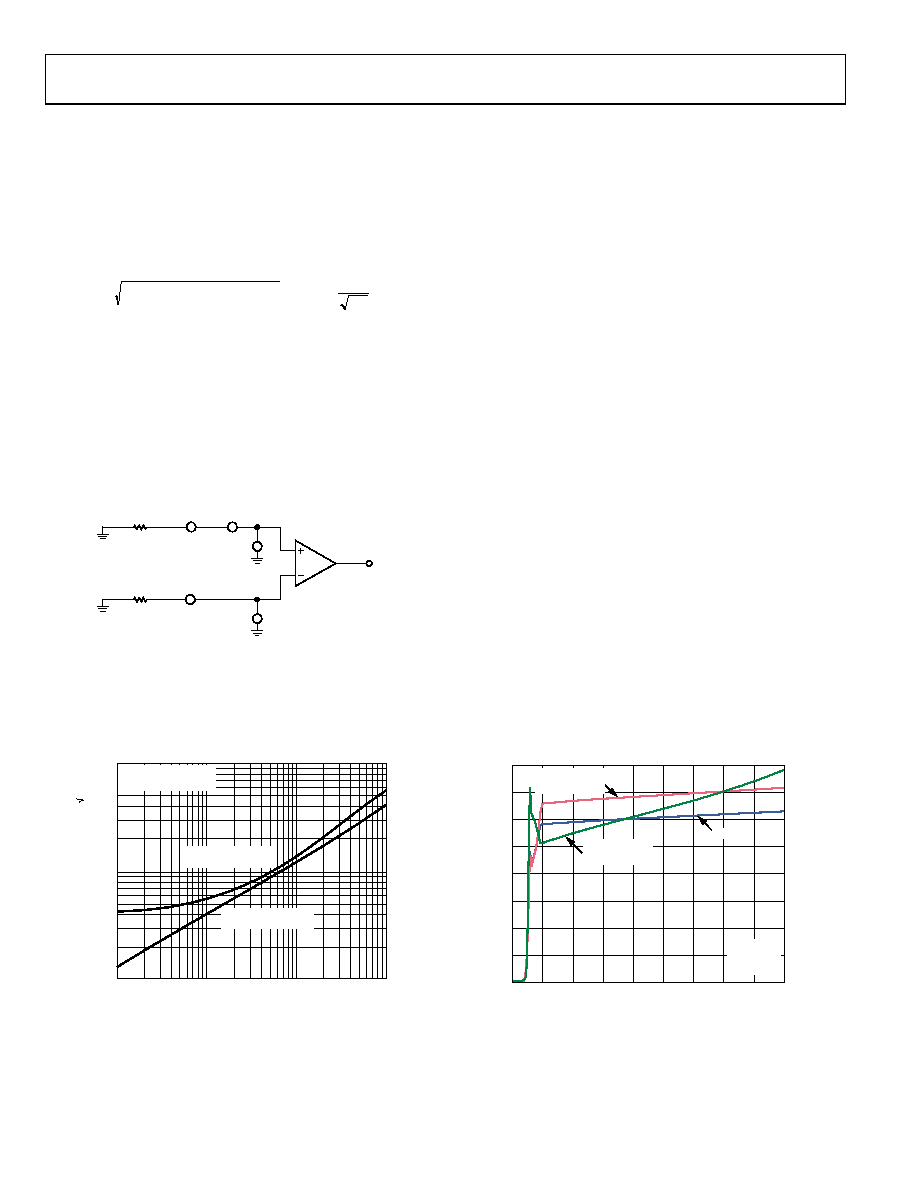
operation. Referring to the op amp noise model circuit configu-
ration illustrated in Figure 82, the expression for an amplifier’s
total equivalent input noise voltage for a source resistance level,
RS, is given by
2
)
(
)
(
)
(
2
nOA
S
nOA
nR
nT
e
R
i
, units in
Hz
V
where:
RS
= 2R, the effective, or equivalent, circuit source resistance.
(enR)2
is the source resistance thermal noise voltage power (4kTR).
k
is the Boltzmann’s constant, 1.38 × 10⁻²³ J/K.
T
is the ambient temperature in Kelvin of the circuit, 273.15 +
TA (°C).
(inOA)2 is the op amp equivalent input noise current spectral
power (1 Hz bandwidth).
(enOA)2 is the op amp equivalent input noise voltage spectral
power (1 Hz bandwidth).
enR
enOA
inOA
R
NOISELESS
R
NOISELESS
0
8237-
0
76
IDEAL
NOISELESS
OP AMP
RS = 2R
Figure 82. Op Amp Noise Circuit Model Used to Determine Total Circuit
Equivalent Input Noise Voltage and Noise Figure
As a design aid, Figure 83 shows the total equivalent input noise
of the ADA4084-2 and the total thermal noise of a resistor for
comparison. Note that for source resistance less than 1 kΩ, the
equivalent input noise voltage of the ADA4084-2 is dominant.
TOTAL SOURCE RESISTANCE, RS ()
100
1
E
Q
U
IV
A
LE
N
T
TH
E
R
M
A
L
N
O
IS
E
(n
V
/
H
z)
10
10k
ADA4084-2 TOTAL
EQUIVALENT NOISE
RESISTOR THERMAL
NOISE ONLY
08
23
7-
07
7
100
1k
100k
FREQUENCY = 1kHz
TA = 25°C
Figure 83. ADA4084-2 Equivalent Thermal Noise vs. Total Source Resistance
Because circuit SNR is the critical parameter in the final analysis,
the noise behavior of a circuit is sometimes expressed in terms
of its noise figure, NF. The noise figure is defined as the ratio of
a circuit’s output signal-to-noise to its input signal-to-noise.
Noise figure is generally used for RF and microwave circuit analysis
in a 50 Ω system. This is not very useful for op amp circuits where
the input and output impedances can vary greatly. For a more
complete description of noise figure, see the MT-052 Tutorial, Op
Amp Noise Figure: Don’t be Mislead
, available at www.analog.com.
Signal levels in the application invariably increase to maximize
circuit SNR, which is not an option in low voltage, single-supply
applications.
Therefore, to achieve optimum circuit SNR in single-supply
applications, it is recommended that an operational amplifier
with the lowest equivalent input noise voltage be chosen, along
with source resistance levels that are consistent with maintaining
low total circuit noise.
COMPARATOR OPERATION
Although op amps are quite different from comparators,
occasionally an unused section of a dual or a quad op amp
can be used as a comparator; however, this is not recommended
for any rail-to-rail output op amps. For rail-to-rail output op
amps, the output stage is generally a ratioed current mirror with
bipolar or MOSFET transistors. With the part operating open
loop, the second stage increases the current drive to the ratioed
mirror to close the loop. However, it cannot, which results in an
increase in supply current. With the op amp configured as a
comparator, the supply current can be significantly higher (see
Figure 84). An unused section should be configured as a voltage
follower with the noninverting input connected to a voltage within
the input voltage range. The ADA4084-2 has unique second
stage and output stage designs that greatly reduce the excess
supply current when the op amp is operating open loop.
800
0
036
S
UP
P
L
Y
C
URRE
NT
(
A)
VSY (V)
0
8237
-078
100
200
300
400
500
600
700
4
8
12
16
20
24
28
32
ADA4084-2
TA = 25°C
RL = ∞
COMPARATOR
OUTPUT LOW
COMPARATOR
OUTPUT HIGH
BUFFER
Figure 84. Supply Current vs. Supply Voltage
相关PDF资料 |
PDF描述 |
|---|---|
| AD708JNZ | IC OPAMP GP DUAL PREC 8DIP |
| LT1112ACN8#PBF | IC PREC OP-AMP LOWPWR DUAL 8-DIP |
| TMM-150-01-S-D | CONN HEADER 100POS DUAL 2MM T/H |
| LT1079CN#PBF | IC PREC OPAMP MICRPWR QUAD 14DIP |
| LT6600IS8-20#PBF | IC AMP DIFF LP FLTR 20MHZ 8-SOIC |
相关代理商/技术参数 |
参数描述 |
|---|---|
| ADA4084-2ARZ_PROMO | 制造商:Analog Devices 功能描述:IC OP AMP 30V SOIC-8 |
| ADA4084-2ARZ-R7 | 功能描述:IC OPAMP GP RRIO 10MHZ DL 8SOIC RoHS:是 类别:集成电路 (IC) >> Linear - Amplifiers - Instrumentation 系列:- 标准包装:1 系列:- 放大器类型:通用 电路数:4 输出类型:满摆幅 转换速率:0.028 V/µs 增益带宽积:105kHz -3db带宽:- 电流 - 输入偏压:3nA 电压 - 输入偏移:100µV 电流 - 电源:3.3µA 电流 - 输出 / 通道:12mA 电压 - 电源,单路/双路(±):2.7 V ~ 12 V,±1.35 V ~ 6 V 工作温度:-40°C ~ 85°C 安装类型:表面贴装 封装/外壳:14-TSSOP(0.173",4.40mm 宽) 供应商设备封装:14-TSSOP 包装:剪切带 (CT) 其它名称:OP481GRUZ-REELCT |
| ADA4084-2ARZ-RL | 功能描述:IC OPAMP GP RRIO 10MHZ DL 8SOIC RoHS:是 类别:集成电路 (IC) >> Linear - Amplifiers - Instrumentation 系列:- 标准包装:1 系列:- 放大器类型:通用 电路数:4 输出类型:满摆幅 转换速率:0.028 V/µs 增益带宽积:105kHz -3db带宽:- 电流 - 输入偏压:3nA 电压 - 输入偏移:100µV 电流 - 电源:3.3µA 电流 - 输出 / 通道:12mA 电压 - 电源,单路/双路(±):2.7 V ~ 12 V,±1.35 V ~ 6 V 工作温度:-40°C ~ 85°C 安装类型:表面贴装 封装/外壳:14-TSSOP(0.173",4.40mm 宽) 供应商设备封装:14-TSSOP 包装:剪切带 (CT) 其它名称:OP481GRUZ-REELCT |
| ADA4084-4ACPZ-R7 | 功能描述:IC OPAMP RRIO 30V QUAD 16LFCSP 制造商:analog devices inc. 系列:- 包装:剪切带(CT) 零件状态:在售 放大器类型:通用 电路数:4 输出类型:满摆幅 压摆率:4.6 V/μs 增益带宽积:15.9MHz 电流 - 输入偏置:140nA 电压 - 输入失调:40μV 电流 - 电源:625μA 电流 - 输出/通道:30mA 电压 - 电源,单/双(±):3 V ~ 30 V,±1.5 V ~ 15 V 工作温度:-40°C ~ 125°C 安装类型:表面贴装 封装/外壳:16-WQFN 裸露焊盘,CSP 供应商器件封装:16-LFCSP-WQ(4x4) 标准包装:1 |
| ADA4084-4ACPZ-RL | 功能描述:IC OPAMP RRIO 30V QUAD 16LFCSP 制造商:analog devices inc. 系列:- 包装:剪切带(CT) 零件状态:在售 放大器类型:通用 电路数:4 输出类型:满摆幅 压摆率:4.6 V/μs 增益带宽积:15.9MHz 电流 - 输入偏置:140nA 电压 - 输入失调:40μV 电流 - 电源:625μA 电流 - 输出/通道:30mA 电压 - 电源,单/双(±):3 V ~ 30 V,±1.5 V ~ 15 V 工作温度:-40°C ~ 125°C 安装类型:表面贴装 封装/外壳:16-WQFN 裸露焊盘,CSP 供应商器件封装:16-LFCSP-WQ(4x4) 标准包装:1 |
发布紧急采购,3分钟左右您将得到回复。