- 您现在的位置:买卖IC网 > PDF目录2063 > ADA4410-6ACPZ-R2 (Analog Devices Inc)IC VIDEO FILTER SELECT 32-LFCSP PDF资料下载
参数资料
| 型号: | ADA4410-6ACPZ-R2 |
| 厂商: | Analog Devices Inc |
| 文件页数: | 6/16页 |
| 文件大小: | 0K |
| 描述: | IC VIDEO FILTER SELECT 32-LFCSP |
| 标准包装: | 1 |
| 类型: | 视频滤波器 |
| 应用: | 录音机,机顶盒 |
| 安装类型: | 表面贴装 |
| 封装/外壳: | 32-LFCSP |
| 供应商设备封装: | 32-LFCSP-EP(5x5) |
| 包装: | 标准包装 |
| 其它名称: | ADA4410-6ACPZ-R2DKR |
ADA4410-6
Rev. B | Page 14 of 16
As previously discussed, the composite video output is
developed by passively summing the Y and C outputs that have
passed through their respective output gain stages, then multiplying
this sum by a factor of two to obtain the output (see Figure 1).
The offset of this output is equal to 2× that of the other outputs.
Because of this, in many cases, it is necessary to ac-couple the
CV output or ensure that it is connected to an input that is ac-
coupled. This is generally not an issue because it is common
practice to employ ac coupling on composite video inputs.
The maximum differential voltage that can be applied across the
LEVEL1 and LEVEL2 inputs is ±500 mV. From a single-ended
standpoint, the LEVEL1 and LEVEL2 inputs have the same
range as the filter inputs. See the Specifications tables for the
limits. The LEVEL1 and LEVEL2 inputs must each be bypassed
to GND with a 0.1 μF ceramic capacitor.
In single-supply applications, a positive output offset must be
applied to keep the negative-most excursions of the output
signals above the specified minimum output swing limit.
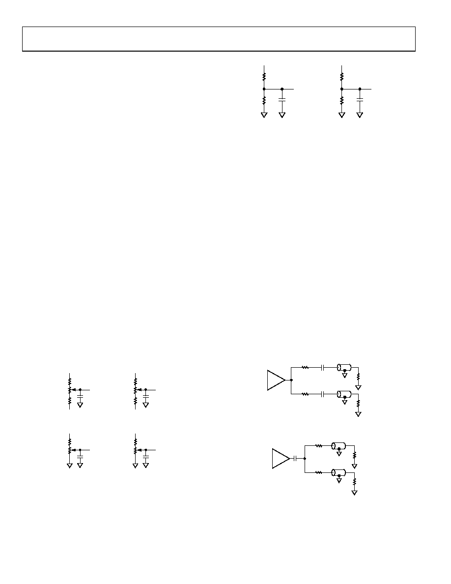
LEVEL1 and LEVEL2 inputs. Figure 23 shows an example of
how to generate fully adjustable LEVEL1 and LEVEL2 voltages
from ±5 V and single +5 V supplies. These circuits show a
general case, but a more practical approach is to fix one voltage
and vary the other. Figure 24 illustrates an effective way to
produce a 600 mV output offset voltage in a single-supply
application. Although the LEVEL2 input could simply be
connected to GND, Figure 24 includes bypassed resistive
voltage dividers for each input so that the input levels can be
changed, if necessary. Additionally, many in-circuit testers
require that I/O signals not be tied directly to the supplies or
GND. DNP indicates do not populate.
0
526
5-
0
48
DUAL SUPPLY
0.1F
LEVEL1
9.53k
1k
9.53k
+5V
–5V
0.1F
LEVEL2
9.53k
1k
9.53k
+5V
–5V
SINGLE SUPPLY
0.1F
LEVEL1
1k
9.09k
+5V
0.1F
LEVEL2
1k
9.09k
+5V
Figure 23. Generating Fully Adjustable Output Offsets
05265-
049
0.1
μF
LEVEL1
634
Ω
10k
Ω
+5V
DNP
LEVEL2
0
Ω
DNP
+5V
Figure 24. Flexible Circuits to Set the LEVEL1 and LEVEL2 Inputs to Obtain
a 600 mV Output Offset on a Single Supply (G = ×2)
INPUT AND OUTPUT COUPLING
Inputs to the ADA4410-6 are normally dc-coupled. Ac coupling
the inputs is not recommended; however, if ac coupling is
necessary, suitable circuitry must be provided following the ac
coupling element to provide proper dc level and bias currents at
the ADA4410-6 input stages.
The ADA4410-6 outputs can be either ac- or dc-coupled. As
discussed in the Output DC Offset Control section, the CV
output offset is different from the other outputs, and the CV
output is generally ac-coupled.
When driving single ac-coupled loads in standard 75 Ω video
distribution systems, 220 μF coupling capacitors are recommended
for use on all but the chrominance signal output. Because the
chrominance signal is a narrow-band modulated carrier, it has
no low frequency content and can therefore be coupled with a
0.1 μF capacitor.
There are two ac coupling options when driving two loads from
one output. One is to simply use the same value capacitor on
the second load, while the other is to use a common coupling
capacitor that is at least twice the value used for the single load
(see Figure 25 and Figure 26).
0
52
65
-05
4
75
CABLE
75
CABLE
220F
75
Figure 25. Driving Two AC-Coupled Loads with Two Coupling Capacitors
05
26
5
-05
5
75
CABLE
75
CABLE
75
470F
Figure 26. Driving Two AC-Coupled Loads with One Common Coupling Capacitor
相关PDF资料 |
PDF描述 |
|---|---|
| ADA4411-3ARQZ | IC HD/FILTER/BUFFER/MUX 24QSOP |
| ADA4412-3ARQZ-R7 | IC FILTER VID RGB/HD/SD 20QSOP |
| ADA4417-3ARMZ | IC VIDEO FILTER TRPL HD 10-MSOP |
| ADA4420-6ARQZ-R7 | IC FILTER VIDEO 6CH HD/SD 16QSOP |
| ADA4430-1YKSZ-RL | IC FILTER VIDEO ULTRA LP SC70-6 |
相关代理商/技术参数 |
参数描述 |
|---|---|
| ADA4410-6ACPZ-R7 | 功能描述:IC VIDEO FILTER SELECT 32-LFCSP RoHS:是 类别:集成电路 (IC) >> 线性 - 视频处理 系列:- 产品变化通告:Product Discontinuation 07/Mar/2011 标准包装:3,000 系列:OMNITUNE™ 类型:调谐器 应用:移动电话,手机,视频显示器 安装类型:表面贴装 封装/外壳:65-WFBGA 供应商设备封装:PG-WFSGA-65 包装:带卷 (TR) 其它名称:SP000365064 |
| ADA4410-6ACPZR7KL1 | 制造商:Analog Devices 功能描述: |
| ADA4410-6ACPZ-RL | 功能描述:IC VIDEO FILTER SELECT 32-LFCSP RoHS:是 类别:集成电路 (IC) >> 线性 - 视频处理 系列:- 产品变化通告:Product Discontinuation 07/Mar/2011 标准包装:3,000 系列:OMNITUNE™ 类型:调谐器 应用:移动电话,手机,视频显示器 安装类型:表面贴装 封装/外壳:65-WFBGA 供应商设备封装:PG-WFSGA-65 包装:带卷 (TR) 其它名称:SP000365064 |
| ADA4411-3 | 制造商:AD 制造商全称:Analog Devices 功能描述:Integrated Triple Video Filter and Buffer with Selectable Cutoff Frequencies and Multiplexed Inputs for RGB, HD/SD |
| ADA4411-3ARQZ | 功能描述:IC HD/FILTER/BUFFER/MUX 24QSOP RoHS:是 类别:集成电路 (IC) >> 线性 - 放大器 - 视频放大器和频缓冲器 系列:- 标准包装:1,000 系列:- 应用:驱动器 输出类型:差分 电路数:3 -3db带宽:350MHz 转换速率:1000 V/µs 电流 - 电源:14.5mA 电流 - 输出 / 通道:60mA 电压 - 电源,单路/双路(±):5 V ~ 12 V,±2.5 V ~ 6 V 安装类型:表面贴装 封装/外壳:20-VFQFN 裸露焊盘 供应商设备封装:20-QFN 裸露焊盘(4x4) 包装:带卷 (TR) |
发布紧急采购,3分钟左右您将得到回复。