- 您现在的位置:买卖IC网 > PDF目录8543 > ADA4411-3ARQZ-RL (Analog Devices Inc)IC HD/FILTER/BUFFER/MUX 24QSOP PDF资料下载
参数资料
| 型号: | ADA4411-3ARQZ-RL |
| 厂商: | Analog Devices Inc |
| 文件页数: | 3/16页 |
| 文件大小: | 0K |
| 描述: | IC HD/FILTER/BUFFER/MUX 24QSOP |
| 标准包装: | 2,500 |
| 应用: | 2:1 多路复用器-放大器 |
| 输出类型: | 满摆幅 |
| 电路数: | 3 |
| 电流 - 电源: | 57mA |
| 电流 - 输出 / 通道: | 30mA |
| 电压 - 电源,单路/双路(±): | 4.5 V ~ 12 V,±2.25 V ~ 6 V |
| 安装类型: | 表面贴装 |
| 封装/外壳: | 24-SSOP(0.154",3.90mm 宽) |
| 供应商设备封装: | 24-QSOP |
| 包装: | 带卷 (TR) |
ADA4411-3
Rev. 0 | Page 11 of 16
APPLICATIONS
OVERVIEW
CUTOFF FREQUENCY SELECTION
With its high impedance multiplexed inputs and high output
drive, the ADA4411-3 is ideally suited to video reconstruction
and antialias filtering applications. The high impedance inputs
give designers flexibility with regard to how the input signals
are terminated. Devices with DAC current source outputs that
feed the ADA4411-3 can be loaded in whatever resistance
provides the best performance, and devices with voltage outputs
can be optimally terminated as well. The ADA4411-3 outputs
can each drive up to two source-terminated 75 Ω loads and can
therefore directly drive the outputs from set-top boxes, DVD
players, and the like without the need for a separate output
buffer.
Four combinations of cutoff frequencies are provided for the
video signals. The cutoff frequencies have been selected to
correspond with the most commonly deployed component
video scanning systems. Selection between the cutoff frequency
combinations is controlled by the logic signals applied to the
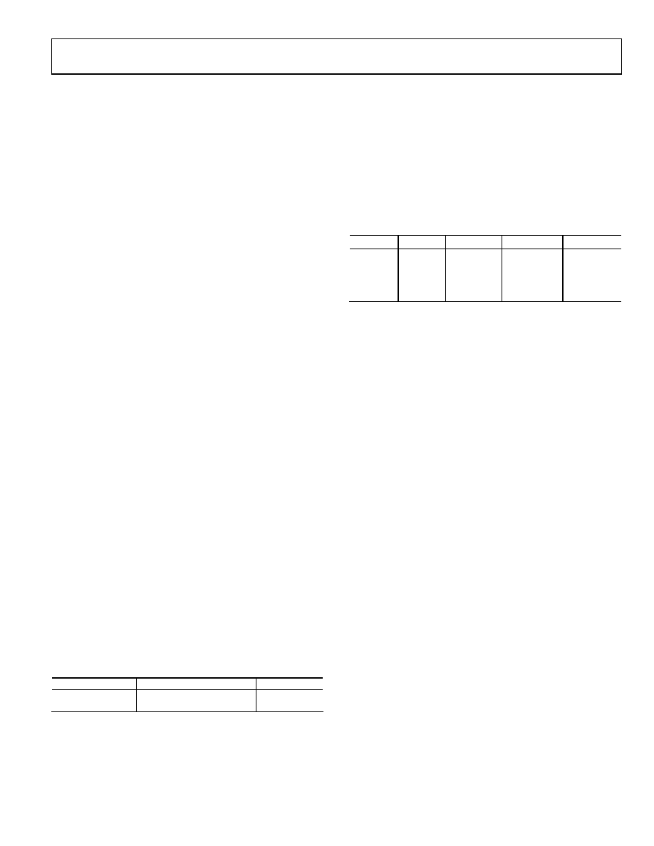
F_SEL_A and F_SEL_B inputs. Table 7 summarizes cutoff
frequency selection.
Table 7. Filter Cutoff Frequency Selection
F_SEL_A
F_SEL_B
Y/G Cutoff
Pb/B Cutoff
Pr/R Cutoff
0
36 MHz
Binary control inputs are provided to select cutoff frequency,
throughput gain, and input signal. These inputs are compatible
with 3 V and 5 V TTL and CMOS logic levels referenced to
GND. The disable feature is asserted by pulling the DISABLE
pin to the positive supply.
The LEVEL1 and LEVEL2 inputs comprise a differential input
that controls the dc level at the output pins.
MULTIPLEXER SELECT INPUTS
Selection between the two multiplexer inputs is controlled by
the logic signals applied to the MUX inputs. Table 6
summarizes the multiplexer operation.
THROUGHPUT GAIN
The throughput gain of the ADA4411-3 signal paths can
be either × 2 or × 4. Gain selection is controlled by the logic
signal applied to the G_SEL pin. Table 6 summarizes how the
gain is selected.
DISABLE
The ADA4411-3 includes a disable feature that can be used
to save power when a particular device is not in use. As
indicated in the Overview section, the disable feature is
asserted by pulling the DISABLE pin to the positive supply.
Table 6 summarizes the disable feature operation. The
DISABLE pin also functions as a reference level for the logic
inputs and therefore must be connected to ground when the
device is not disabled.
Table 6. Logic Pin Function Description
DISABLE
MUX
G_SEL
VS+ = Disabled
1 = Channel 1 Selected
1 = ×2 Gain
GND = Enabled
0 = Channel 2 Selected
0 = ×4 Gain
0
1
36 MHz
18 MHz
1
0
18 MHz
1
9 MHz
OUTPUT DC OFFSET CONTROL
The LEVEL1 and LEVEL2 inputs work as a differential, input-
referred output offset control. In other words, the output offset
voltage of a given channel is equal to the difference in voltage
between the LEVEL1 and LEVEL2 inputs, multiplied by the
overall filter gain. This relationship is expressed in Equation 1.
(1)
)
)(
(
)
(
G
LEVEL
OUT
VOS
2
1
=
LEVEL1 and LEVEL2 are the voltages applied to the respective
inputs, and G is the throughput gain.
For example, with the G_SEL input set for ×2 gain, setting
LEVEL1 to 300 mV and LEVEL2 to 0 V shifts the offset voltages
at the ADA4411-3 outputs to 600 mV. This particular setting
can be used in most single-supply applications to keep the
output swings safely above the negative supply rail.
The maximum differential voltage that can be applied across the
LEVEL1 and LEVEL2 inputs is ±500 mV. From a single-ended
standpoint, the LEVEL1 and LEVEL2 inputs have the same
range as the filter inputs. See the Specifications tables for the
limits. The LEVEL1 and LEVEL2 inputs must each be bypassed
to GND with a 0.1 μF ceramic capacitor.
In single-supply applications, a positive output offset must be
applied to keep the negative-most excursions of the output
signals above the specified minimum output swing limit.
相关PDF资料 |
PDF描述 |
|---|---|
| LT6207IGN#TR | IC OPAMP VID QUAD 100MHZ 16-SSOP |
| VE-B3B-MU-F2 | CONVERTER MOD DC/DC 95V 200W |
| 1838420-2 | CONN MALE M12 4POS STR BLACK |
| LT6207IGN#PBF | IC OPAMP VID QUAD 100MHZ 16-SSOP |
| 1838418-2 | CONN MALE M12 4POS STR BLACK |
相关代理商/技术参数 |
参数描述 |
|---|---|
| ADA4412-3 | 制造商:AD 制造商全称:Analog Devices 功能描述:Integrated Triple Video Filter with Selectable Cutoff Frequencies for RGB, HD/SD |
| ADA4412-3ARQZ | 功能描述:IC FILTER VID RGB/HD/SD 20-QSOP RoHS:是 类别:集成电路 (IC) >> 线性 - 视频处理 系列:- 标准包装:250 系列:- 类型:电平移位器 应用:LCD 电视机/监控器 安装类型:表面贴装 封装/外壳:28-WFQFN 裸露焊盘 供应商设备封装:28-WQFN(4x4)裸露焊盘 包装:带卷 (TR) 其它名称:296-32523-2TPS65198RUYT-ND |
| ADA4412-3ARQZ-R7 | 功能描述:IC FILTER VID RGB/HD/SD 20QSOP RoHS:是 类别:集成电路 (IC) >> 线性 - 视频处理 系列:- 产品变化通告:Product Discontinuation 07/Mar/2011 标准包装:3,000 系列:OMNITUNE™ 类型:调谐器 应用:移动电话,手机,视频显示器 安装类型:表面贴装 封装/外壳:65-WFBGA 供应商设备封装:PG-WFSGA-65 包装:带卷 (TR) 其它名称:SP000365064 |
| ADA4412-3ARQZ-RL | 功能描述:IC FILTER VID RGB/HD/SD 20QSOP RoHS:是 类别:集成电路 (IC) >> 线性 - 视频处理 系列:- 产品变化通告:Product Discontinuation 07/Mar/2011 标准包装:3,000 系列:OMNITUNE™ 类型:调谐器 应用:移动电话,手机,视频显示器 安装类型:表面贴装 封装/外壳:65-WFBGA 供应商设备封装:PG-WFSGA-65 包装:带卷 (TR) 其它名称:SP000365064 |
| ADA4417-3 | 制造商:AD 制造商全称:Analog Devices 功能描述:Integrated Triple Video Filter for High Definition Video |
发布紧急采购,3分钟左右您将得到回复。