参数资料
| 型号: | ADA4638-1ARZ |
| 厂商: | Analog Devices Inc |
| 文件页数: | 10/25页 |
| 文件大小: | 0K |
| 描述: | IC OPAMP RRO ZERO DRIFT 8SOIC |
| 标准包装: | 98 |
| 放大器类型: | 零漂移 |
| 电路数: | 1 |
| 输出类型: | 满摆幅 |
| 转换速率: | 1.5 V/µs |
| 增益带宽积: | 1.5MHz |
| -3db带宽: | 2.5MHz |
| 电流 - 输入偏压: | 45pA |
| 电压 - 输入偏移: | 0.5µV |
| 电流 - 电源: | 850µA |
| 电流 - 输出 / 通道: | 38mA |
| 电压 - 电源,单路/双路(±): | 4.5 V ~ 30 V,±2.25 V ~ 15 V |
| 工作温度: | -40°C ~ 125°C |
| 安装类型: | 表面贴装 |
| 封装/外壳: | 8-SOIC(0.154",3.90mm 宽) |
| 供应商设备封装: | 8-SO |
| 包装: | 管件 |
Data Sheet
ADA4638-1
Rev. 0 | Page 17 of 24
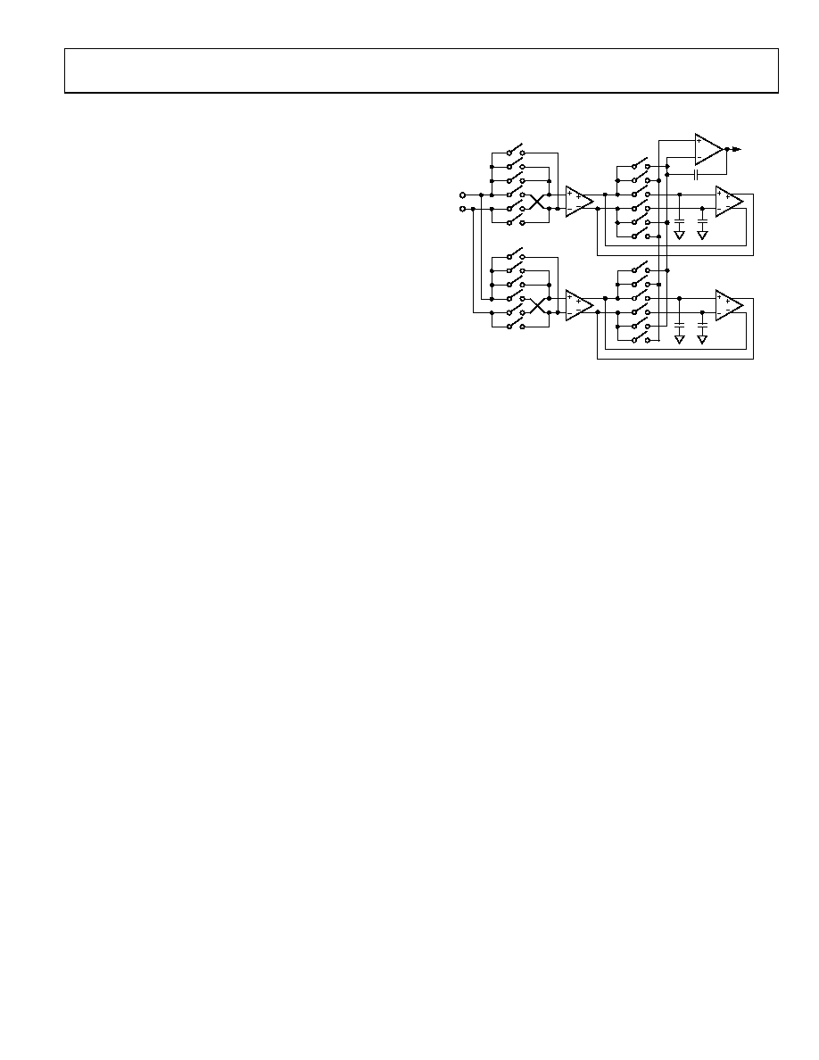
THEORY OF OPERATION
noninverting and inverting amplifier inputs are +IN and –IN,
respectively. The transconductance amplifiers, A1 and A2, are
the two input gain stages; the A3 and A4 transconductance
amplifiers are the nulling amplifiers used to correct the offsets
of A1 and A2, and AOUT is the output amplifier. A four-phase
cycle (φ1 to φ4) controls the switches. In Phase 1 (φ1), A1 is
auto-zeroed where both the inputs of A1 are connected to +IN.
A1 produces a differential output current of VOS1 × gm1, where
VOS1 is the input offset voltage of A1, and gm1 is the differential
transconductance of A1. The outputs of A1 are then connected
to the inputs and outputs of A3. A3 is designed to have an
equivalent resistance of 1/gm3, where gm3 is the transconduct-
ance of A3. The amplified version of VOS1, which is VOS1 ×
gm1/gm3, is stored on Capacitors C1 and C2. These capacitors,
together with A3, are used to null out the offset of A1 when A1
amplifies the signal during the φ3 and φ4 phases.
While A1 is being auto-zeroed, A2 (nulled by A4, C3, and C4)
is used for signal amplification. The ADA4638-1 differs from
traditional auto-zero amplifiers in that the input offset voltage
is also chopped during signal amplification. During φ1, +IN
and IN are applied to the noninverting and inverting inputs,
respectively, of A2. However, during φ2, both the inputs and
outputs of A2 are inverted, and the input offset voltage of A2 is
chopped.
The combination of auto-zeroing and chopping offers two major
benefits. First, any residual offset following the auto-zeroing
process is reduced. During φ1, the output offset voltage of A2 is
+VOSAZ2 and during φ2, it is –VOSAZ2, producing a theoretical
average of zero. Second, the aliased noise spectrum density at dc
due to auto-zeroing is modulated up to the chopping frequency,
and the prechopped noise spectrum density at the chopping
frequency is modulated down to dc. This noise transformation
lowers the noise spectrum density at dc, thus making zero-drift
amplifiers ideal for low frequency signal amplification.
During φ3 and φ4, the roles of A1 and A2 are reversed. A2
offset is nulled, and the input signal is chopped and amplified
using A1.
+IN
–IN
A1
Ф4
Ф3
Ф1
Ф2
Ф1
Ф3
Ф1
Ф3
Ф2
Ф1
Ф2
Ф1
Ф3
Ф1
Ф4
Ф3
Ф4
Ф1
Ф3
Ф4
A2
A3
C1
C2
C3
C4
AOUT
CC
OUT
A4
1007
2-
15
7
Figure 57. ADA4638-1 Amplifier Block Diagram
INPUT PROTECTION
The ADA4638-1 has internal ESD protection diodes that are
connected between the inputs and each supply rail. These diodes
protect the input transistors in the event of electrostatic dis-
charge and are reverse-biased during normal operation. However,
if either input exceeds one of the supply rails, these ESD diodes
become forward-biased and large amounts of current begin to
flow through them. Without current limiting, this excessive
fault current causes permanent damage to the device. If the
inputs are expected to be subject to overvoltage conditions,
insert a resistor in series with each input to limit the input
current to 10 mA maximum. However, consider the resistor
thermal noise effect on the entire circuit.
NO OUTPUT PHASE REVERSAL
An undesired phenomenon, phase reversal (also known as
phase inversion) occurs in many amplifiers when one or both of
the inputs are driven beyond the specified input common-mode
voltage range, in effect reversing the polarity of the output. In
some cases, phase reversal can induce lockups and cause
equipment damage as well as self destruction.
The ADA4638-1 has been carefully designed to prevent any
output phase reversal, provided that both inputs are maintained
within the supply voltages. If either one or both inputs may
exceed either supply voltage, place resistors in series with the
inputs to limit the current to less than 10 mA.
The ADA4638-1 features rail-to-rail output with a supply volt-
age from 4.5 V to 30 V. Figure 58 shows the input and output
waveforms of the ADA4638-1 configured as a unity-gain buffer
with a supply voltage of ±15 V and a resistive load of 10 kΩ.
The ADA4638-1 does not exhibit phase reversal.
相关PDF资料 |
PDF描述 |
|---|---|
| N3793-5202RB | CONN HEADER 10PS R/A SHORT LATCH |
| AD8205YRZ | IC AMP DIFF 8SOIC |
| AD8616ARZ | IC OPAMP GP R-R CMOS 24MHZ 8SOIC |
| N3793-6202RB | CONN HEADER 10PS STR SHORT LATCH |
| RMCF2512FT12R0 | RES TF 12 OHM 1% 1W 2512 |
相关代理商/技术参数 |
参数描述 |
|---|---|
| ADA4638-1ARZ_PROMO | 制造商:Analog Devices 功能描述:IC OP AMP PREC RRO SOIC-8 |
| ADA4638-1ARZ-R7 | 功能描述:IC OPAMP RRO ZERO DRIFT 8SOIC RoHS:是 类别:集成电路 (IC) >> Linear - Amplifiers - Instrumentation 系列:- 标准包装:1,000 系列:- 放大器类型:电压反馈 电路数:4 输出类型:满摆幅 转换速率:33 V/µs 增益带宽积:20MHz -3db带宽:30MHz 电流 - 输入偏压:2nA 电压 - 输入偏移:3000µV 电流 - 电源:2.5mA 电流 - 输出 / 通道:30mA 电压 - 电源,单路/双路(±):4.5 V ~ 16.5 V,±2.25 V ~ 8.25 V 工作温度:-40°C ~ 85°C 安装类型:表面贴装 封装/外壳:14-SOIC(0.154",3.90mm 宽) 供应商设备封装:14-SOIC 包装:带卷 (TR) |
| ADA4638-1ARZ-RL | 功能描述:IC OPAMP RRO ZERO DRIFT 8SOIC RoHS:是 类别:集成电路 (IC) >> Linear - Amplifiers - Instrumentation 系列:- 标准包装:1,000 系列:- 放大器类型:电压反馈 电路数:4 输出类型:满摆幅 转换速率:33 V/µs 增益带宽积:20MHz -3db带宽:30MHz 电流 - 输入偏压:2nA 电压 - 输入偏移:3000µV 电流 - 电源:2.5mA 电流 - 输出 / 通道:30mA 电压 - 电源,单路/双路(±):4.5 V ~ 16.5 V,±2.25 V ~ 8.25 V 工作温度:-40°C ~ 85°C 安装类型:表面贴装 封装/外壳:14-SOIC(0.154",3.90mm 宽) 供应商设备封装:14-SOIC 包装:带卷 (TR) |
| ADA-4643 | 制造商:Avago Technologies 功能描述:AMP RF SI 4643 SOT-343-4 3.5V 制造商:Avago Technologies 功能描述:AMP, RF SI, 4643, SOT-343-4, 3.5V |
| ADA-4643-BLK | 制造商:AGILENT 制造商全称:AGILENT 功能描述:Silicon Bipolar Darlington Amplifier |
发布紧急采购,3分钟左右您将得到回复。