- 您现在的位置:买卖IC网 > PDF目录2139 > ADA4817-1ACPZ-RL (Analog Devices Inc)IC OPAMP VF 410MHZ LN 8LFCSP PDF资料下载
参数资料
| 型号: | ADA4817-1ACPZ-RL |
| 厂商: | Analog Devices Inc |
| 文件页数: | 24/28页 |
| 文件大小: | 0K |
| 描述: | IC OPAMP VF 410MHZ LN 8LFCSP |
| 标准包装: | 5,000 |
| 系列: | FastFET™ |
| 放大器类型: | 电压反馈 |
| 电路数: | 1 |
| 转换速率: | 870 V/µs |
| 增益带宽积: | 410MHz |
| -3db带宽: | 1.05GHz |
| 电流 - 输入偏压: | 2pA |
| 电压 - 输入偏移: | 400µV |
| 电流 - 电源: | 19mA |
| 电流 - 输出 / 通道: | 40mA |
| 电压 - 电源,单路/双路(±): | 5 V ~ 10 V,±2.5 V ~ 5 V |
| 工作温度: | -40°C ~ 105°C |
| 安装类型: | 表面贴装 |
| 封装/外壳: | 8-VFDFN 裸露焊盘,CSP |
| 供应商设备封装: | 8-LFCSP-VD(3x3) |
| 包装: | 带卷 (TR) |
第1页第2页第3页第4页第5页第6页第7页第8页第9页第10页第11页第12页第13页第14页第15页第16页第17页第18页第19页第20页第21页第22页第23页当前第24页第25页第26页第27页第28页
Data Sheet
ADA4817-1/ADA4817-2
Rev. B | Page 5 of 28
ABSOLUTE MAXIMUM RATINGS
Table 3.
Parameter
Rating
Supply Voltage
10.6 V
Power Dissipation
Common-Mode Input Voltage
VS 0.5 V to +VS + 0.5 V
Differential Input Voltage
±VS
Storage Temperature Range
65°C to +125°C
Operating Temperature Range
40°C to +105°C
Lead Temperature (Soldering, 10 sec)
300°C
Junction Temperature
150°C
Stresses above those listed under Absolute Maximum Ratings
may cause permanent damage to the device. This is a stress
rating only; functional operation of the device at these or any
other conditions above those indicated in the operational
section of this specification is not implied. Exposure to absolute
maximum rating conditions for extended periods may affect
device reliability.
THERMAL RESISTANCE
θJA is specified for the worst-case conditions, that is, θJA is
specified for a device soldered in the circuit board for the
surface-mount packages.
Table 4.
Package Type
θJA
θJC
Unit
LFCSP_VD (ADA4817-1)
94
29
°C/W
SOIC_N_EP (ADA4817-1)
79
29
°C/W
LFCSP_WQ (ADA4817-2)
64
14
°C/W
MAXIMUM SAFE POWER DISSIPATION
The maximum safe power dissipation for the ADA4817-1/
ADA4817-2 are limited by the associated rise in junction
temperature (TJ) on the die. At approximately 150°C (which is
the glass transition temperature), the properties of the plastic
change. Even temporarily exceeding this temperature limit may
change the stresses that the package exerts on the die, permanently
shifting the parametric performance of the ADA4817-x. Exceeding
a junction temperature of 175°C for an extended period can result
in changes in silicon devices, potentially causing degradation or
loss of functionality.
The power dissipated in the package (PD) is the sum of the
quiescent power dissipation and the power dissipated in the
die due to the ADA4817-1/ADA4817-2 drive at the output.
The quiescent power is the voltage between the supply pins (VS)
multiplied by the quiescent current (IS).
PD = Quiescent Power + (Total Drive Power – Load Power) (1)
(
)
L
OUT
L
OUT
S
D
R
V
R
V
I
V
P
2
–
2
×
+
×
=
(2)
Consider RMS output voltages. If RL is referenced to VS, as
in single-supply operation, the total drive power is VS × IOUT. If
the rms signal levels are indeterminate, consider the worst-case
scenario, when VOUT = VS/4 for RL to midsupply.
(
) (
)
L
S
D
R
V
I
V
P
2
4
/
+
×
=
(3)
In single-supply operation with RL referenced to VS, the worst-
case situation is VOUT = VS/2.
Airflow increases heat dissipation, effectively reducing θJA.
More metal directly in contact with the package leads and
exposed paddle from metal traces, throughholes, ground,
and power planes also reduces θJA.
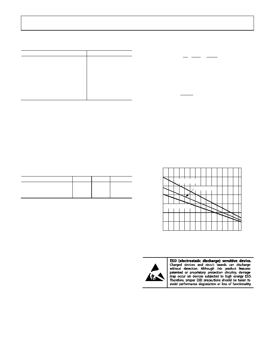
Figure 4 shows the maximum safe power dissipation in the
package vs. the ambient temperature for the exposed paddle
LFCSP_VD (single 94°C/W), SOIC_N_EP (single 79°C/W)
and LFCSP_WQ (dual 64°C/W) package on a JEDEC standard
4-layer board. θJA values are approximations.
3.5
0
–40
AMBIENT TEMPERATURE (°C)
MA
XI
MU
M
PO
W
ER
D
ISSI
PA
T
IO
N
(W
)
3.0
2.5
2.0
1.5
1.0
0.5
–30 –20 –10
0
10
20
30
40
50
60
70
80
90 100
ADA4817-1, LFCSP
ADA4817-2, LFCSP
07756-
008
ADA4817-1, SOIC
Figure 4. Maximum Safe Power Dissipation vs. Ambient Temperature for
a 4-Layer Board
ESD CAUTION
相关PDF资料 |
PDF描述 |
|---|---|
| ADA4830-1BCPZ-R7 | IC AMP BATT PROTECT 8LFCSP |
| ADA4830-2BCPZ-R7 | IC AMP BATT PROTECT DUAL 16LFCSP |
| ADA4841-2YRZ-R7 | IC OPAMP VF R-R DUAL LP LN 8SOIC |
| ADA4850-2YCPZ-R2 | IC OPAMP VF R-R DUAL 16LFCSP |
| ADA4851-4YRUZ | IC OPAMP VF R-R QUAD LP 14TSSOP |
相关代理商/技术参数 |
参数描述 |
|---|---|
| ADA4817-1ARD-EBZ | 功能描述:BOARD EVAL FOR ADA4817 SOIC RoHS:是 类别:编程器,开发系统 >> 评估板 - 运算放大器 系列:- 产品培训模块:Lead (SnPb) Finish for COTS Obsolescence Mitigation Program 标准包装:1 系列:- |
| ADA4817-1ARDZ | 功能描述:IC OPAMP VF 410MHZ LN 40MA 8SOIC RoHS:是 类别:集成电路 (IC) >> Linear - Amplifiers - Instrumentation 系列:FastFET™ 标准包装:2,500 系列:- 放大器类型:通用 电路数:4 输出类型:- 转换速率:0.6 V/µs 增益带宽积:1MHz -3db带宽:- 电流 - 输入偏压:45nA 电压 - 输入偏移:2000µV 电流 - 电源:1.4mA 电流 - 输出 / 通道:40mA 电压 - 电源,单路/双路(±):3 V ~ 32 V,±1.5 V ~ 16 V 工作温度:0°C ~ 70°C 安装类型:表面贴装 封装/外壳:14-TSSOP(0.173",4.40mm 宽) 供应商设备封装:14-TSSOP 包装:带卷 (TR) 其它名称:LM324ADTBR2G-NDLM324ADTBR2GOSTR |
| ADA4817-1ARDZ-R7 | 功能描述:IC OPAMP VF 410MHZ LN 40MA 8SOIC RoHS:是 类别:集成电路 (IC) >> Linear - Amplifiers - Instrumentation 系列:FastFET™ 标准包装:1 系列:- 放大器类型:通用 电路数:4 输出类型:满摆幅 转换速率:0.028 V/µs 增益带宽积:105kHz -3db带宽:- 电流 - 输入偏压:3nA 电压 - 输入偏移:100µV 电流 - 电源:3.3µA 电流 - 输出 / 通道:12mA 电压 - 电源,单路/双路(±):2.7 V ~ 12 V,±1.35 V ~ 6 V 工作温度:-40°C ~ 85°C 安装类型:表面贴装 封装/外壳:14-TSSOP(0.173",4.40mm 宽) 供应商设备封装:14-TSSOP 包装:剪切带 (CT) 其它名称:OP481GRUZ-REELCT |
| ADA4817-1ARDZ-RL | 功能描述:IC OPAMP VF 410MHZ LN 40MA 8SOIC RoHS:是 类别:集成电路 (IC) >> Linear - Amplifiers - Instrumentation 系列:FastFET™ 标准包装:1 系列:- 放大器类型:通用 电路数:4 输出类型:满摆幅 转换速率:0.028 V/µs 增益带宽积:105kHz -3db带宽:- 电流 - 输入偏压:3nA 电压 - 输入偏移:100µV 电流 - 电源:3.3µA 电流 - 输出 / 通道:12mA 电压 - 电源,单路/双路(±):2.7 V ~ 12 V,±1.35 V ~ 6 V 工作温度:-40°C ~ 85°C 安装类型:表面贴装 封装/外壳:14-TSSOP(0.173",4.40mm 宽) 供应商设备封装:14-TSSOP 包装:剪切带 (CT) 其它名称:OP481GRUZ-REELCT |
| ADA4817-2 | 制造商:AD 制造商全称:Analog Devices 功能描述:Low Noise, 1 GHz FastFET Op Amps |
发布紧急采购,3分钟左右您将得到回复。