- 您现在的位置:买卖IC网 > PDF目录5280 > ADA4841-1YRJZ-RL (Analog Devices Inc)IC OPAMP VF R-R LP LN SOT23-6 PDF资料下载
参数资料
| 型号: | ADA4841-1YRJZ-RL |
| 厂商: | Analog Devices Inc |
| 文件页数: | 6/21页 |
| 文件大小: | 0K |
| 描述: | IC OPAMP VF R-R LP LN SOT23-6 |
| 标准包装: | 10,000 |
| 放大器类型: | 电压反馈 |
| 电路数: | 1 |
| 输出类型: | 满摆幅 |
| 转换速率: | 13 V/µs |
| -3db带宽: | 80MHz |
| 电流 - 输入偏压: | 3µA |
| 电压 - 输入偏移: | 40µV |
| 电流 - 电源: | 1.5mA |
| 电流 - 输出 / 通道: | 60mA |
| 电压 - 电源,单路/双路(±): | 2.7 V ~ 12 V,±1.35 V ~ 6 V |
| 工作温度: | -40°C ~ 125°C |
| 安装类型: | 表面贴装 |
| 封装/外壳: | SOT-23-6 |
| 供应商设备封装: | SOT-23-6 |
| 包装: | 带卷 (TR) |
ADA4841-1/ADA4841-2
Rev. E | Page 13 of 20
THEORY OF OPERATION
AMPLIFIER DESCRIPTION
The ADA4841-1/ADA4841-2 are low power, low noise,
precision voltage-feedback op amps for single or dual voltage
supply operation. The ADA4841-1/ADA4841-2 are fabricated
on ADI’s second generation XFCB process and feature trimmed
supply current and offset voltage. The 2.1 nV/√Hz voltage noise
(very low for a 1.1 mA supply current amplifier), 40 μV offset
voltage, and sub 1 μV/°C offset drift is accomplished with an
input stage made of an undegenerated PNP input pair driving a
symmetrical folded cascode. A rail-to-rail output stage provides
the maximum linear signal range possible on low voltage
supplies and has the current drive capability needed for the
relatively low resistance feedback networks required for low
noise operation. CMRR, PSRR, and open-loop gain are all
typically above 100 dB, preserving the precision performance in
a variety of configurations. Gain bandwidth is kept high for this
power level to preserve the outstanding linearity performance
for frequencies up to 100 kHz. The ADA4841-1 has a power-
down function to further reduce power consumption. All this
results in a low noise, power efficient, precision amplifier that is
well-suited for high resolution and precision applications.
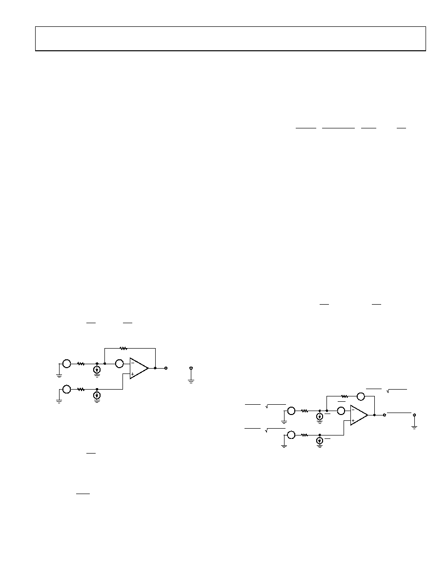
DC ERRORS
Figure 39 shows a typical connection diagram and the major dc
error sources. The ideal transfer function (all error sources set
to 0 and infinite dc gain) can be written as
IN
G
F
IP
G
F
OUT
V
R
V
R
V
×
×
+
= 1
(1)
05614-
004
RG
– VIN +
RS
– VIP +
IB+
IB–
+ VOUT –
RF
+ VOS –
Figure 39. Typical Connection Diagram and DC Error Sources
This reduces to the familiar forms for inverting and
noninverting op amp gain expressions
IP
G
F
OUT
V
R
V
×
+
= 1
(2)
(Noninverting gain, VIN = 0 V)
IN
G
F
OUT
V
R
V
×
=
(3)
(Inverting gain, VIP = 0 V)
The total output voltage error is the sum of errors due to the
amplifier offset voltage and input currents. The output error
due to the offset voltage can be estimated as
+
×
+
+
=
G
F
OUT
PNOM
P
OFFSET
OUT
R
A
V
PSRR
V
CMRR
VCM
V
NOM
ERROR
1
(4)
where:
NOM
OFFSET
V
is the offset voltage at the specified supply voltage.
This is measured with the input and output at midsupply.
VCM is the common-mode voltage.
VP is the power supply voltage.
NOM
p
V
is the specified power supply voltage.
CMRR is the common-mode rejection ratio.
PSRR is the power supply rejection ratio.
A is the dc open-loop gain.
The output error due to the input currents can be estimated as
+
×
+
×
+
×
=
B
G
F
S
B
G
F
G
F
OUT
I
R
I
R
V
ERROR
1
)
||
(
(5)
Note that setting RS equal to RF||RG compensates for the voltage
error due to the input bias current.
NOISE CONSIDERATIONS
Figure 40 illustrates the primary noise contributors for the
typical gain configurations. The total rms output noise is
the root-mean-square of all the contributions.
0
56
14-
0
05
RG
RS
ien
+ vout_en –
RF
ven
4kT × RS
vn _ RS =
4kT × RG
vn _ RG =
4kT × RF
vn _ RF =
Figure 40. Noise Sources in Typical Connection
相关PDF资料 |
PDF描述 |
|---|---|
| LPPB101NFSC-RC | CONN HEADER .050" 10POS SMD GOLD |
| NPPN062GFNS-RC | CONN RECEPT 2MM DUAL SMD 12POS |
| ADA4051-1AKSZ-R2 | IC OPAMP RRIO ZERO DRIFT SC70-5 |
| NPPN052GFNP-RC | CONN RECEPT 2MM DUAL SMD 10POS |
| NPPN082AFCN-RC | CONN RECEPT 2MM DUAL STR 16POS |
相关代理商/技术参数 |
参数描述 |
|---|---|
| ADA4841-1YRZ | 制造商:Analog Devices 功能描述:OP Amp Single Volt Fdbk R-R O/P ±6V/12V 8-Pin SOIC N T/R 制造商:Analog Devices 功能描述:LOW POWER, LOW NOISE AND DISTORTION, RAIL-TO-RAIL OUTPUT AMP - Rail/Tube 制造商:Rochester Electronics LLC 功能描述: |
| ADA4841-1YRZ-R7 | 功能描述:IC OPAMP VF R-R LP LN 60MA 8SOIC RoHS:是 类别:集成电路 (IC) >> Linear - Amplifiers - Instrumentation 系列:- 产品培训模块:Differential Circuit Design Techniques for Communication Applications 标准包装:1 系列:- 放大器类型:RF/IF 差分 电路数:1 输出类型:差分 转换速率:9800 V/µs 增益带宽积:- -3db带宽:2.9GHz 电流 - 输入偏压:3µA 电压 - 输入偏移:- 电流 - 电源:40mA 电流 - 输出 / 通道:- 电压 - 电源,单路/双路(±):3 V ~ 3.6 V 工作温度:-40°C ~ 85°C 安装类型:表面贴装 封装/外壳:16-VQFN 裸露焊盘,CSP 供应商设备封装:16-LFCSP-VQ 包装:剪切带 (CT) 产品目录页面:551 (CN2011-ZH PDF) 其它名称:ADL5561ACPZ-R7CT |
| ADA4841-1YRZ-R7 | 制造商:Analog Devices 功能描述:IC OP-AMP 80MHZ 13V/S SOIC-8 |
| ADA4841-1YRZ-RL | 功能描述:IC OPAMP VF R-R LP LN 60MA 8SOIC RoHS:是 类别:集成电路 (IC) >> Linear - Amplifiers - Instrumentation 系列:- 标准包装:50 系列:- 放大器类型:通用 电路数:2 输出类型:满摆幅 转换速率:1.8 V/µs 增益带宽积:6.5MHz -3db带宽:4.5MHz 电流 - 输入偏压:5nA 电压 - 输入偏移:100µV 电流 - 电源:65µA 电流 - 输出 / 通道:35mA 电压 - 电源,单路/双路(±):1.8 V ~ 5.25 V,±0.9 V ~ 2.625 V 工作温度:-40°C ~ 85°C 安装类型:表面贴装 封装/外壳:10-TFSOP,10-MSOP(0.118",3.00mm 宽) 供应商设备封装:10-MSOP 包装:管件 |
| ADA4841-2 | 制造商:AD 制造商全称:Analog Devices 功能描述:Low Power, Low Noise and Distortion ail-to-Rail Output Amplifiers |
发布紧急采购,3分钟左右您将得到回复。