- 您现在的位置:买卖IC网 > PDF目录5454 > ADA4850-2YCPZ-RL (Analog Devices Inc)IC OPAMP VF R-R DUAL 16LFCSP PDF资料下载
参数资料
| 型号: | ADA4850-2YCPZ-RL |
| 厂商: | Analog Devices Inc |
| 文件页数: | 14/17页 |
| 文件大小: | 0K |
| 描述: | IC OPAMP VF R-R DUAL 16LFCSP |
| 标准包装: | 5,000 |
| 放大器类型: | 电压反馈 |
| 电路数: | 2 |
| 输出类型: | 满摆幅 |
| 转换速率: | 220 V/µs |
| -3db带宽: | 175MHz |
| 电流 - 输入偏压: | 2.3µA |
| 电压 - 输入偏移: | 600µV |
| 电流 - 电源: | 2.5mA |
| 电流 - 输出 / 通道: | 118mA |
| 电压 - 电源,单路/双路(±): | 2.7 V ~ 6 V |
| 工作温度: | -40°C ~ 125°C |
| 安装类型: | 表面贴装 |
| 封装/外壳: | 16-VFQFN 裸露焊盘,CSP |
| 供应商设备封装: | 16-LFCSP-VQ |
| 包装: | 带卷 (TR) |
Data Sheet
ADA4850-1/ADA4850-2
Rev. C | Page 5 of 16
ABSOLUTE MAXIMUM RATINGS
Table 3.
Parameter
Rating
Supply Voltage
12.6 V
Power Dissipation
Power Down Pin Voltage
(V
S + 6) V
Common-Mode Input Voltage
(V
S 0.5 ) V to (+VS + 0.5) V
Differential Input Voltage
+V
S to VS
Storage Temperature
65°C to +125°C
Operating Temperature Range
40°C to +125°C
Lead Temperature Range
(Soldering 10 sec)
300°C
Junction Temperature
150°C
Stresses above those listed under Absolute Maximum Ratings
may cause permanent damage to the device. This is a stress
rating only; functional operation of the device at these or any
other conditions above those indicated in the operational
section of this specification is not implied. Exposure to absolute
maximum rating conditions for extended periods may affect
device reliability.
THERMAL RESISTANCE
θJA is specified for the worst-case conditions, that is, θJA is
specified for the device soldered in the circuit board for
surface-mount packages.
Table 4.
Package Type
θ
JA
Unit
16-Lead LFCSP
72.8
°C/W
8-Lead LFCSP
80
°C/W
Maximum Power Dissipation
The maximum safe power dissipation for the ADA4850-1/
ADA4850-2 is limited by the associated rise in junction
temperature (TJ) on the die. At approximately 150°C, which
is the glass transition temperature, the plastic changes its
properties. Even temporarily exceeding this temperature limit
may change the stresses that the package exerts on the die,
permanently shifting the parametric performance of the
ADA4850-1/ADA4850-2. Exceeding a junction temperature
of 150°C for an extended period of time can result in changes
in silicon devices, potentially causing degradation or loss of
functionality.
The power dissipated in the package (PD) is the sum of the quies-
cent power dissipation and the power dissipated in the die due
to the ADA4850-1/ADA4850-2 drive at the output. The
quiescent power is the voltage between the supply pins (VS)
times the quiescent current (IS).
PD = Quiescent Power + (Total Drive Power Load Power)
(
)
L
OUT
L
OUT
S
D
R
V
R
V
I
V
P
2
×
+
×
=
RMS output voltages should be considered. If RL is referenced
to VS, as in single-supply operation, the total drive power is
VS × IOUT. If the rms signal levels are indeterminate, consider
the worst case, when VOUT = VS/4 for RL to midsupply.
(
) ( )
L
S
D
R
4
V
I
V
P
2
/
+
×
=
In single-supply operation with RL referenced to VS, the worst
case is VOUT = VS/2.
Airflow increases heat dissipation, effectively reducing θJA.
Also, more metal directly in contact with the package leads and
exposed paddle from metal traces through holes, ground, and
power planes reduce θJA.
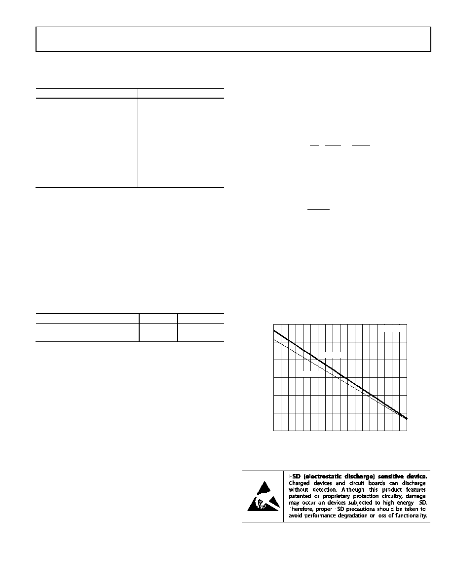
Figure 4 shows the maximum safe power dissipation in the
package vs. the ambient temperature for the LFCSP (91°C/W)
package on a JEDEC standard 4-layer board. θJA values are
approximations.
Figure 4. Maximum Power Dissipation vs. Temperature for a 4-Layer Board
ESD CAUTION
–55
125
–45 –35 –25 –15 –5
5
15 25 35 45 55 65 75 85 95 105 115
MA
XI
MU
M
PO
W
ER
D
ISSI
PA
T
IO
N
(W
)
AMBIENT TEMPERATURE (
°C)
05320-
055
0
3.0
2.5
2.0
1.5
1.0
0.5
LFCSP-8
LFCSP-16
TJ = 150°C
相关PDF资料 |
PDF描述 |
|---|---|
| TSW-144-05-L-D | CONN HEADER 88POS .100" DL GOLD |
| TSW-145-05-L-D | CONN HEADER 90POS .100" DL GOLD |
| AD8646ARZ-REEL7 | IC OPAMP GP R-R 24MHZ DUAL 8SOIC |
| TSW-146-05-L-D | CONN HEADER 92POS .100" DL GOLD |
| 51761-10002410AALF | RA STB REC PWRBLADE F/G |
相关代理商/技术参数 |
参数描述 |
|---|---|
| ADA4850-2YCPZ-RL7 | 功能描述:IC OPAMP VF R-R DUAL 16LFCSP RoHS:是 类别:集成电路 (IC) >> Linear - Amplifiers - Instrumentation 系列:- 标准包装:160 系列:- 放大器类型:通用 电路数:4 输出类型:满摆幅 转换速率:10 V/µs 增益带宽积:9MHz -3db带宽:- 电流 - 输入偏压:1pA 电压 - 输入偏移:250µV 电流 - 电源:730µA 电流 - 输出 / 通道:28mA 电压 - 电源,单路/双路(±):2.7 V ~ 5.5 V,±1.35 V ~ 2.75 V 工作温度:-40°C ~ 125°C 安装类型:表面贴装 封装/外壳:16-SOIC(0.154",3.90mm 宽) 供应商设备封装:16-SOIC N 包装:管件 |
| ADA4851-1 | 制造商:AD 制造商全称:Analog Devices 功能描述:Low Cost, High Speed, Rail-to-Rail, Output Op Amps |
| ADA4851-1_06 | 制造商:AD 制造商全称:Analog Devices 功能描述:Low Cost, High Speed, Rail-to-Rail, Output Op Amps |
| ADA4851-1_07 | 制造商:AD 制造商全称:Analog Devices 功能描述:Low Cost, High Speed, Rail-to-Rail, Output Op Amps |
| ADA4851-1ARJ | 制造商:Analog Devices 功能描述:LOW COST, HIGH-SPEED RAIL-TO-RAIL OUTPUT OP AMP - Bulk |
发布紧急采购,3分钟左右您将得到回复。