- 您现在的位置:买卖IC网 > PDF目录2139 > ADA4855-3YCPZ-R7 (Analog Devices Inc)IC OPAMP VF R-R TRPL LP 16LFCSP PDF资料下载
参数资料
| 型号: | ADA4855-3YCPZ-R7 |
| 厂商: | Analog Devices Inc |
| 文件页数: | 9/20页 |
| 文件大小: | 0K |
| 描述: | IC OPAMP VF R-R TRPL LP 16LFCSP |
| 标准包装: | 1 |
| 放大器类型: | 电压反馈 |
| 电路数: | 3 |
| 输出类型: | 满摆幅 |
| 转换速率: | 870 V/µs |
| -3db带宽: | 410MHz |
| 电流 - 输入偏压: | 3.8µA |
| 电压 - 输入偏移: | 1300µV |
| 电流 - 电源: | 7.8mA |
| 电流 - 输出 / 通道: | 57mA |
| 电压 - 电源,单路/双路(±): | 3 V ~ 5.5 V |
| 工作温度: | -40°C ~ 105°C |
| 安装类型: | 表面贴装 |
| 封装/外壳: | 16-VQFN 裸露焊盘,CSP |
| 供应商设备封装: | 16-LFCSP-VQ EP(4x4) |
| 包装: | 标准包装 |
| 产品目录页面: | 768 (CN2011-ZH PDF) |
| 其它名称: | ADA4855-3YCPZ-R7DKR |
Data Sheet
ADA4855-3
Rev. A | Page 17 of 20
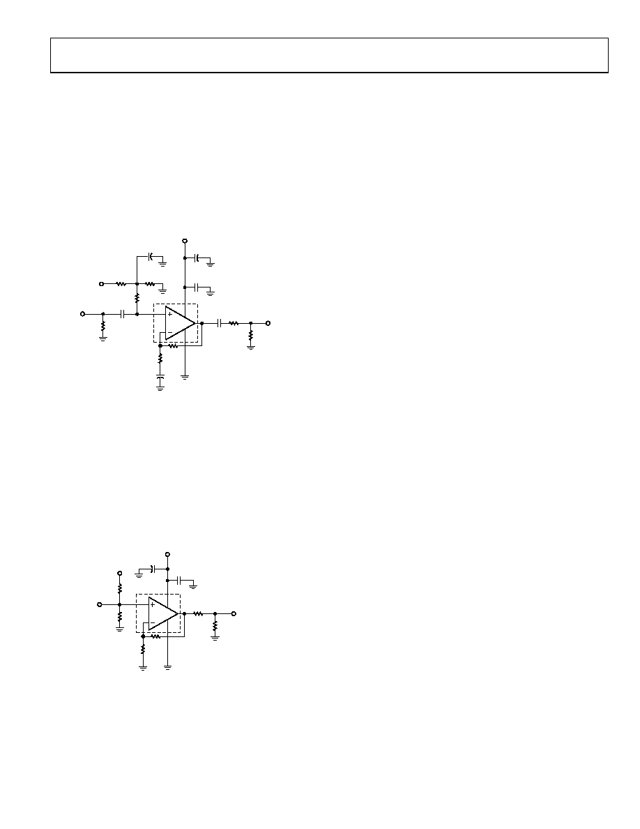
SINGLE-SUPPLY OPERATION
The ADA4855-3 is designed for a single power supply. Figure 54
shows the schematic for a single 5 V supply video driver. The
input signal is ac-coupled into the amplifier via C1. Resistor R2
and Resistor R4 establish the input midsupply reference for the
amplifier. C5 prevents constant current from being drawn
through the gain set resistor. C6 is the output coupling capacitor.
For more information on ac-coupled single-supply operation of
op amps, see Avoiding Op-Amp Instability Problems in Single-
Supply Applications, Analog Dialogue, Volume 35, Number 2,
March-May, 2001, at www.analog.com.
07
68
5-
15
5
C2
1F
R2
50k
R4
50k
R3
1k
C1
22F
U1
R1
75
R5
1k
R6
1k
C6
220F
R7
75
R8
75
C5
22F
ADA4855-3
5V
VOUT
VIN
–VS
C3
10F
C4
0.01F
5V
Figure 54. AC-Coupled, Single-Supply Video Driver Schematic
Another way to configure the ADA4855-3 in single-supply
operation is dc-coupled. The common-mode input voltage can
go ~200 mV below ground, which makes it a true single-supply
amplifier. However, in video applications, the black level is set at
0 V, which means that the output of the amplifier must go to
ground level as well. The ADA4855-3 has a rail-to-rail output
that can swing to within 100 mV from either rail. Figure 55
shows the schematic for adding 50 mV dc offset to the input
signal so that the output is not clipped while still properly
terminating the input with 75 Ω.
07
68
5-
15
6
R1
3.74k
U1
R2
76.8
R3
1k
R4
1k
R5
75
R6
75
ADA4855-3
5V
VOUT
VIN
–VS
C1
10F
C2
0.1F
5V
Figure 55. DC-Coupled, Single-Supply Video Driver Schematic
POWER SUPPLY BYPASSING
Careful attention must be paid to bypassing the power supply
pins of the ADA4855-3. High quality capacitors with low
equivalent series resistance (ESR), such as multilayer ceramic
capacitors (MLCCs), should be used to minimize supply voltage
ripple and power dissipation. A large, usually tantalum, 2.2 μF
to 47 μF capacitor located in close proximity to the ADA4855-3
is required to provide good decoupling for lower frequency
signals. The actual value is determined by the circuit transient
and frequency requirements. In addition, 0.1 μF MLCC decoupling
capacitors should be located as close to each of the power supply
pins and across both supplies as is physically possible, no more
than 1/8-inch away. The ground returns should terminate
immediately into the ground plane. Locating the bypass capacitor
return close to the load return minimizes ground loops and
improves performance.
LAYOUT
As is the case with all high speed applications, careful attention
to printed circuit board (PCB) layout details prevents associated
board parasitics from becoming problematic. The ADA4855-3
can operate at up to 410 MHz; therefore, proper RF design
techniques must be employed. The PCB should have a ground
plane covering all unused portions of the component side of the
board to provide a low impedance return path. Removing the
ground plane on all layers from the area near and under the
input and output pins reduces stray capacitance. Signal lines
connecting the feedback and gain resistors should be kept as short
as possible to minimize the inductance and stray capacitance
associated with these traces. Termination resistors and loads
should be located as close as possible to their respective inputs
and outputs. Input and output traces should be kept as far apart
as possible to minimize coupling (crosstalk) through the board.
Adherence to microstrip or stripline design techniques for long
signal traces (greater than 1 inch) is recommended. For more
information on high speed board layout, see A Practical Guide
to High-Speed Printed-Circuit-Board Layout, Analog Dialogue,
Volume 39, September 2005, at www.analog.com.
相关PDF资料 |
PDF描述 |
|---|---|
| ADA4857-2YCPZ-RL | IC OPAMP VF DUAL ULDIST 16LFCSP |
| ADA4858-3ACPZ-R7 | IC OPAMP CF TRPL LP 21MA 16LFCSP |
| ADA4860-1YRJZ-RL | IC OPAMP CF LP 85MA SOT23-6 |
| ADA4861-3YRZ-RL7 | IC OPAMP CF TRPL LP 100MA 14SOIC |
| ADA4891-3ARUZ | IC OPAMP GP R-R CMOS 14TSSOP |
相关代理商/技术参数 |
参数描述 |
|---|---|
| ADA4855-3YCPZ-RL | 功能描述:IC OPAMP VF R-R TRPL LP 16LFCSP RoHS:是 类别:集成电路 (IC) >> Linear - Amplifiers - Instrumentation 系列:- 标准包装:1,000 系列:- 放大器类型:电压反馈 电路数:4 输出类型:满摆幅 转换速率:33 V/µs 增益带宽积:20MHz -3db带宽:30MHz 电流 - 输入偏压:2nA 电压 - 输入偏移:3000µV 电流 - 电源:2.5mA 电流 - 输出 / 通道:30mA 电压 - 电源,单路/双路(±):4.5 V ~ 16.5 V,±2.25 V ~ 8.25 V 工作温度:-40°C ~ 85°C 安装类型:表面贴装 封装/外壳:14-SOIC(0.154",3.90mm 宽) 供应商设备封装:14-SOIC 包装:带卷 (TR) |
| ADA4856-3 | 制造商:AD 制造商全称:Analog Devices 功能描述:Single-Supply, High Speed, Fixed G = +2, Rail-to-Rail Output Video Amplifier |
| ADA4856-3YCP-EBZ | 功能描述:BOARD EVAL FOR ADA4856-3YCP RoHS:是 类别:编程器,开发系统 >> 评估演示板和套件 系列:* 标准包装:1 系列:- 主要目的:电信,线路接口单元(LIU) 嵌入式:- 已用 IC / 零件:IDT82V2081 主要属性:T1/J1/E1 LIU 次要属性:- 已供物品:板,电源,线缆,CD 其它名称:82EBV2081 |
| ADA4856-3YCPZ-R2 | 功能描述:IC AMP 3CH RRO VFB G=+2 16LFCSP RoHS:是 类别:集成电路 (IC) >> 线性 - 放大器 - 视频放大器和频缓冲器 系列:- 标准包装:1,000 系列:- 应用:驱动器 输出类型:差分 电路数:3 -3db带宽:350MHz 转换速率:1000 V/µs 电流 - 电源:14.5mA 电流 - 输出 / 通道:60mA 电压 - 电源,单路/双路(±):5 V ~ 12 V,±2.5 V ~ 6 V 安装类型:表面贴装 封装/外壳:20-VFQFN 裸露焊盘 供应商设备封装:20-QFN 裸露焊盘(4x4) 包装:带卷 (TR) |
| ADA4856-3YCPZ-R7 | 功能描述:IC AMP 3CH RRO VFB G=2 16LFCSP RoHS:是 类别:集成电路 (IC) >> 线性 - 放大器 - 视频放大器和频缓冲器 系列:- 产品培训模块:Lead (SnPb) Finish for COTS Obsolescence Mitigation Program 标准包装:50 系列:- 应用:TFT-LCD 面板:VCOM 驱动器 输出类型:满摆幅 电路数:1 -3db带宽:35MHz 转换速率:40 V/µs 电流 - 电源:3.7mA 电流 - 输出 / 通道:1.3A 电压 - 电源,单路/双路(±):9 V ~ 20 V,±4.5 V ~ 10 V 安装类型:表面贴装 封装/外壳:8-TSSOP,8-MSOP(0.118",3.00mm 宽)裸露焊盘 供应商设备封装:8-uMax-EP 包装:管件 |
发布紧急采购,3分钟左右您将得到回复。