参数资料
| 型号: | ADA4891-3ARUZ |
| 厂商: | Analog Devices Inc |
| 文件页数: | 8/24页 |
| 文件大小: | 0K |
| 描述: | IC OPAMP GP R-R CMOS 14TSSOP |
| 标准包装: | 96 |
| 放大器类型: | 通用 |
| 电路数: | 3 |
| 输出类型: | 满摆幅 |
| 转换速率: | 210 V/µs |
| -3db带宽: | 240MHz |
| 电流 - 输入偏压: | 2pA |
| 电压 - 输入偏移: | 2500µV |
| 电流 - 电源: | 4.4mA |
| 电流 - 输出 / 通道: | 125mA |
| 电压 - 电源,单路/双路(±): | 2.7 V ~ 5.5 V,±1.35 V ~ 2.75 V |
| 工作温度: | -40°C ~ 125°C |
| 安装类型: | 表面贴装 |
| 封装/外壳: | 14-TSSOP(0.173",4.40mm 宽) |
| 供应商设备封装: | 14-TSSOP |
| 包装: | 管件 |
ADA4891-1/ADA4891-2/ADA4891-3/ADA4891-4
Data Sheet
Rev. E | Page 16 of 24
Table 6. Recommended Component Values and Effect of Gain on ADA4891-3/ADA4891-4 Performance (RL = 1 k)
Feedback Network Values
3 dB Small-Signal Bandwidth (MHz)
Slew Rate (V/s)
Peaking (dB)
Gain
RF ()
RG ()
VOUT = 200 mV p-p
tR
tF
1
453
97
186
194
0.9
+1
0
Open
220
151
262
4.1
+2
453
97
181
223
0.9
+5
453
90.6
31
112
120
0
+10
453
45.3
13
68
67
0
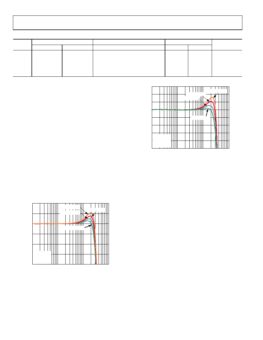
EFFECT OF RF ON 0.1 dB GAIN FLATNESS
Gain flatness is an important specification in video applications.
It represents the maximum allowable deviation in the signal
amplitude within the pass band. Tests have revealed that the
human eye is unable to distinguish brightness variations of
less than 1%, which translates into a 0.1 dB signal drop within
the pass band or, put simply, 0.1 dB gain flatness.
The PCB layout configuration and bond pads of the chip often
contribute to stray capacitance. The stray capacitance at the
inverting input forms a pole with the feedback and gain resistors.
This additional pole adds phase shift and reduces phase margin
in the closed-loop phase response, causing instability in the
amplifier and peaking in the frequency response.
Figure 52 and Figure 53 show the effect of using various values
for Feedback Resistor RF on the 0.1 dB gain flatness of the parts.
Figure 52 shows the effect for the ADA4891-1/ADA4891-2.
Figure 53 show the effect for the ADA4891-3/ADA4891-4.
Note that a larger RF value causes more peaking because the
additional pole formed by RF and the input stray capacitance
shifts down in frequency and interacts significantly with the
internal poles of the amplifier.
–0.4
–0.3
–0.2
–0.1
0
0.1
0.2
1
0.1
10
100
FREQUENCY (MHz)
N
OR
M
A
LIZE
D
C
LOS
E
D
-LOO
P
G
AI
N
(
d
B)
VS = 5V
G = +2
VOUT = 2V p-p
RL = 150Ω
RG = RF = 604
RG = RF = 549
RG = RF = 649
RG = RF = 698
08054-
022
Figure 52. 0.1 dB Gain Flatness, Noninverting Gain Configuration,
ADA4891-1/ADA4891-2
–0.4
–0.5
–0.3
–0.2
–0.1
0
0.1
0.2
0.3
1
0.1
10
100
FREQUENCY (MHz)
N
OR
M
A
LIZE
D
C
LOS
E
D
-LOO
P
G
AI
N
(
d
B)
08054-
085
VS = 5V
G = +2
VOUT = 2V p-p
RL = 150Ω
RG = RF = 453
RG = RF = 402
RG = RF = 357
RG = RF = 301
Figure 53. 0.1 dB Gain Flatness, Noninverting Gain Configuration,
ADA4891-3/ADA4891-4
To obtain the desired 0.1 dB bandwidth, adjust the feedback
be adjusted, a small capacitor can be placed in parallel with RF
to reduce peaking.
The feedback capacitor, CF, forms a zero with the feedback
resistor, which cancels out the pole formed by the input stray
capacitance and the gain and feedback resistors. For a first pass
in determining the CF value, use the following equation:
RG × CS = RF × CF
where:
RG is the gain resistor.
CS is the input stray capacitance.
RF is the feedback resistor.
CF is the feedback capacitor.
Using this equation, the original closed-loop frequency response of
the amplifier is restored, as if there is no stray input capacitance.
Most often, however, the value of CF is determined empirically.
Figure 54 shows the effect of using various values for the
feedback capacitor to reduce peaking. In this case, the
ADA4891-1/ ADA4891-2 are used for demonstration purposes
and RF = RG = 604 Ω. The input stray capacitance, together with
the board parasitics, is approximately 2 pF.
相关PDF资料 |
PDF描述 |
|---|---|
| ADA4896-2ACPZ-RL | IC OPAMP GP R-R 50MHZ LP 8LFCSP |
| ADA4898-1YRDZ-RL | IC OPAMP VF ULN ULDIST 8SOIC |
| ADA4899-1YRDZ-R7 | IC OPAMP VF ULN ULDIST 8SOIC |
| ADA4927-2YCPZ-R2 | IC OPAMP CF DIFF DUAL LN 24LFCSP |
| ADA4930-1YCPZ-R2 | IC DIFF AMP 1.35GHZ 16-LFCSP |
相关代理商/技术参数 |
参数描述 |
|---|---|
| ADA4891-3ARUZ_PROMO | 制造商:Analog Devices 功能描述:OP-AMP 220MHZ 210V/US 2.5MV |
| ADA4891-3ARUZ-R7 | 功能描述:IC OPAMP GP R-R CMOS 14TSSOP RoHS:是 类别:集成电路 (IC) >> Linear - Amplifiers - Instrumentation 系列:- 标准包装:2,500 系列:- 放大器类型:通用 电路数:1 输出类型:满摆幅 转换速率:0.11 V/µs 增益带宽积:350kHz -3db带宽:- 电流 - 输入偏压:4nA 电压 - 输入偏移:20µV 电流 - 电源:260µA 电流 - 输出 / 通道:20mA 电压 - 电源,单路/双路(±):2.7 V ~ 36 V,±1.35 V ~ 18 V 工作温度:-40°C ~ 85°C 安装类型:表面贴装 封装/外壳:8-SOIC(0.154",3.90mm 宽) 供应商设备封装:8-SO 包装:带卷 (TR) |
| ADA4891-3ARUZ-RL | 功能描述:IC OPAMP GP R-R CMOS 14TSSOP RoHS:是 类别:集成电路 (IC) >> Linear - Amplifiers - Instrumentation 系列:- 标准包装:160 系列:- 放大器类型:通用 电路数:4 输出类型:满摆幅 转换速率:10 V/µs 增益带宽积:9MHz -3db带宽:- 电流 - 输入偏压:1pA 电压 - 输入偏移:250µV 电流 - 电源:730µA 电流 - 输出 / 通道:28mA 电压 - 电源,单路/双路(±):2.7 V ~ 5.5 V,±1.35 V ~ 2.75 V 工作温度:-40°C ~ 125°C 安装类型:表面贴装 封装/外壳:16-SOIC(0.154",3.90mm 宽) 供应商设备封装:16-SOIC N 包装:管件 |
| ADA4891-3ARZ | 制造商:Analog Devices 功能描述:Tube 制造商:Analog Devices 功能描述:OP Amp Triple GP R-R O/P 5.5V 14-Pin SOIC N Tube |
| ADA4891-3ARZ-R7 | 功能描述:IC OPAMP GP R-R CMOS 14SOIC RoHS:是 类别:集成电路 (IC) >> Linear - Amplifiers - Instrumentation 系列:- 标准包装:2,500 系列:- 放大器类型:通用 电路数:1 输出类型:满摆幅 转换速率:0.11 V/µs 增益带宽积:350kHz -3db带宽:- 电流 - 输入偏压:4nA 电压 - 输入偏移:20µV 电流 - 电源:260µA 电流 - 输出 / 通道:20mA 电压 - 电源,单路/双路(±):2.7 V ~ 36 V,±1.35 V ~ 18 V 工作温度:-40°C ~ 85°C 安装类型:表面贴装 封装/外壳:8-SOIC(0.154",3.90mm 宽) 供应商设备封装:8-SO 包装:带卷 (TR) |
发布紧急采购,3分钟左右您将得到回复。