- 您现在的位置:买卖IC网 > PDF目录5406 > ADA4891-4ARUZ-R7 (Analog Devices Inc)IC OPAMP GP R-R CMOS 14TSSOP PDF资料下载
参数资料
| 型号: | ADA4891-4ARUZ-R7 |
| 厂商: | Analog Devices Inc |
| 文件页数: | 21/24页 |
| 文件大小: | 0K |
| 描述: | IC OPAMP GP R-R CMOS 14TSSOP |
| 标准包装: | 1,000 |
| 放大器类型: | 通用 |
| 电路数: | 4 |
| 输出类型: | 满摆幅 |
| 转换速率: | 210 V/µs |
| -3db带宽: | 240MHz |
| 电流 - 输入偏压: | 2pA |
| 电压 - 输入偏移: | 2500µV |
| 电流 - 电源: | 4.4mA |
| 电流 - 输出 / 通道: | 125mA |
| 电压 - 电源,单路/双路(±): | 2.7 V ~ 5.5 V,±1.35 V ~ 2.75 V |
| 工作温度: | -40°C ~ 125°C |
| 安装类型: | 表面贴装 |
| 封装/外壳: | 14-TSSOP(0.173",4.40mm 宽) |
| 供应商设备封装: | 14-TSSOP |
| 包装: | 带卷 (TR) |
ADA4891-1/ADA4891-2/ADA4891-3/ADA4891-4
Data Sheet
Rev. E | Page 6 of 24
ABSOLUTE MAXIMUM RATINGS
Table 3.
Parameter
Rating
Supply Voltage
6 V
Input Voltage (Common Mode)
VS 0.5 V to +VS
Differential Input Voltage
±VS
Storage Temperature Range
65°C to +125°C
Operating Temperature Range
40°C to +125°C
Lead Temperature (Soldering, 10 sec)
300°C
Stresses above those listed under Absolute Maximum Ratings
may cause permanent damage to the device. This is a stress
rating only; functional operation of the device at these or any
other conditions above those indicated in the operational
section of this specification is not implied. Exposure to absolute
maximum rating conditions for extended periods may affect
device reliability.
MAXIMUM POWER DISSIPATION
The maximum power that can be safely dissipated by the
ADA4891-1/ADA4891-2/ADA4891-3/ADA4891-4 is limited
by the associated rise in junction temperature. The maximum
safe junction temperature for plastic encapsulated devices is
determined by the glass transition temperature of the plastic,
approximately 150°C. Temporarily exceeding this limit can
cause a shift in parametric performance due to a change in the
stresses exerted on the die by the package. Exceeding a junction
temperature of 175°C for an extended period can result in
device failure.
The still-air thermal properties of the package (θJA), the ambient
temperature (TA), and the total power dissipated in the package
(PD) can be used to determine the junction temperature of the die.
The junction temperature can be calculated as
TJ = TA + (PD × θJA)
(1)
The power dissipated in the package (PD) is the sum of the
quiescent power dissipation and the power dissipated in the
package due to the load drive for all outputs. It can be calculated by
PD = (VT × IS) + (VS VOUT) × (VOUT/RL)
(2)
where:
VT is the total supply rail.
IS is the quiescent current.
VS is the positive supply rail.
VOUT is the output of the amplifier.
RL is the output load of the amplifier.
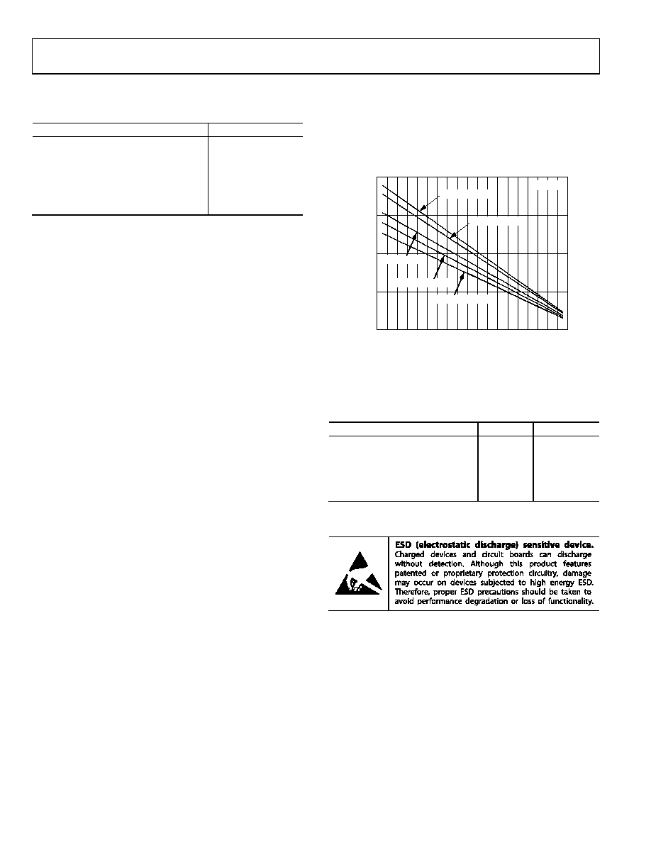
To ensure proper operation, it is necessary to observe the maxi-
mum power derating curves shown in Figure 6. These curves
the maximum safe power dissipation in the package vs. the
ambient temperature on a JEDEC standard 4-layer board.
0
0.5
1.0
2.0
1.5
–55
–35
–15
5
25
45
65
85
105
125
AMBIENT TEMPERATURE (°C)
MA
XI
MU
M
PO
W
ER
D
ISSI
PA
TION
(
W)
14-LEAD TSSOP
8-LEAD SOIC_N
14-LEAD SOIC_N
5-LEAD SOT-23
8-LEAD MSOP
TJ = 150°C
08054-
002
Figure 6. Maximum Power Dissipation vs. Ambient Temperature
ADA4891-2/ADA4891-3/ADA4891-4 package.
Table 4.
Package Type
θJA
Unit
5-Lead SOT-23
146
°C/W
8-Lead SOIC_N
115
°C/W
8-Lead MSOP
133
°C/W
14-Lead SOIC_N
162
°C/W
14-Lead TSSOP
108
°C/W
ESD CAUTION
相关PDF资料 |
PDF描述 |
|---|---|
| 1V5KE180CA | TVS BIDIRECT 180V 1500W DO201AE |
| HDC-S102-31P1-KR | CONN HEADER 102POS 3ROW VERT |
| MMD21-0071R1 | CONN RACK/PANEL 7POS 5A |
| RGH1608-2C-P-470-B | RES 47.0 OHM 1/6W 0.1% 0603 SMD |
| 1V5KE180A | TVS UNIDIRECT 180V 1500W DO201AE |
相关代理商/技术参数 |
参数描述 |
|---|---|
| ADA4891-4ARUZ-RL | 功能描述:IC OPAMP GP R-R CMOS 14TSSOP RoHS:是 类别:集成电路 (IC) >> Linear - Amplifiers - Instrumentation 系列:- 标准包装:2,500 系列:- 放大器类型:通用 电路数:1 输出类型:满摆幅 转换速率:0.11 V/µs 增益带宽积:350kHz -3db带宽:- 电流 - 输入偏压:4nA 电压 - 输入偏移:20µV 电流 - 电源:260µA 电流 - 输出 / 通道:20mA 电压 - 电源,单路/双路(±):2.7 V ~ 36 V,±1.35 V ~ 18 V 工作温度:-40°C ~ 85°C 安装类型:表面贴装 封装/外壳:8-SOIC(0.154",3.90mm 宽) 供应商设备封装:8-SO 包装:带卷 (TR) |
| ADA4891-4ARZ | 功能描述:IC OPAMP GP R-R CMOS 14SOIC RoHS:是 类别:集成电路 (IC) >> Linear - Amplifiers - Instrumentation 系列:- 产品培训模块:Differential Circuit Design Techniques for Communication Applications 标准包装:1 系列:- 放大器类型:RF/IF 差分 电路数:1 输出类型:差分 转换速率:9800 V/µs 增益带宽积:- -3db带宽:2.9GHz 电流 - 输入偏压:3µA 电压 - 输入偏移:- 电流 - 电源:40mA 电流 - 输出 / 通道:- 电压 - 电源,单路/双路(±):3 V ~ 3.6 V 工作温度:-40°C ~ 85°C 安装类型:表面贴装 封装/外壳:16-VQFN 裸露焊盘,CSP 供应商设备封装:16-LFCSP-VQ 包装:剪切带 (CT) 产品目录页面:551 (CN2011-ZH PDF) 其它名称:ADL5561ACPZ-R7CT |
| ADA4891-4ARZ_PROMO | 制造商:Analog Devices 功能描述:OP-AMP 220MHZ 210V/US 3.1MV |
| ADA4891-4ARZ-R7 | 功能描述:IC OPAMP GP R-R CMOS 14SOIC RoHS:是 类别:集成电路 (IC) >> Linear - Amplifiers - Instrumentation 系列:- 标准包装:2,500 系列:- 放大器类型:通用 电路数:1 输出类型:满摆幅 转换速率:0.11 V/µs 增益带宽积:350kHz -3db带宽:- 电流 - 输入偏压:4nA 电压 - 输入偏移:20µV 电流 - 电源:260µA 电流 - 输出 / 通道:20mA 电压 - 电源,单路/双路(±):2.7 V ~ 36 V,±1.35 V ~ 18 V 工作温度:-40°C ~ 85°C 安装类型:表面贴装 封装/外壳:8-SOIC(0.154",3.90mm 宽) 供应商设备封装:8-SO 包装:带卷 (TR) |
| ADA4891-4ARZ-RL | 功能描述:IC OPAMP GP R-R CMOS 14SOIC RoHS:是 类别:集成电路 (IC) >> Linear - Amplifiers - Instrumentation 系列:- 标准包装:2,500 系列:- 放大器类型:通用 电路数:1 输出类型:满摆幅 转换速率:0.11 V/µs 增益带宽积:350kHz -3db带宽:- 电流 - 输入偏压:4nA 电压 - 输入偏移:20µV 电流 - 电源:260µA 电流 - 输出 / 通道:20mA 电压 - 电源,单路/双路(±):2.7 V ~ 36 V,±1.35 V ~ 18 V 工作温度:-40°C ~ 85°C 安装类型:表面贴装 封装/外壳:8-SOIC(0.154",3.90mm 宽) 供应商设备封装:8-SO 包装:带卷 (TR) |
发布紧急采购,3分钟左右您将得到回复。