- 您现在的位置:买卖IC网 > PDF目录5879 > ADA4898-2YRDZ-RL (Analog Devices Inc)IC OPAMP VF 65MHZ DL LN 8SOIC PDF资料下载
参数资料
| 型号: | ADA4898-2YRDZ-RL |
| 厂商: | Analog Devices Inc |
| 文件页数: | 6/20页 |
| 文件大小: | 0K |
| 描述: | IC OPAMP VF 65MHZ DL LN 8SOIC |
| 标准包装: | 2,500 |
| 放大器类型: | 电压反馈 |
| 电路数: | 1 |
| 转换速率: | 55 V/µs |
| -3db带宽: | 65MHz |
| 电流 - 输入偏压: | 100nA |
| 电压 - 输入偏移: | 20µV |
| 电流 - 电源: | 7.9mA |
| 电流 - 输出 / 通道: | 40mA |
| 电压 - 电源,单路/双路(±): | ±4.5 V ~ 16.5 V |
| 工作温度: | -40°C ~ 105°C |
| 安装类型: | 表面贴装 |
| 封装/外壳: | 8-SOIC(0.154",3.90mm Width)裸露焊盘 |
| 供应商设备封装: | 8-SOIC-EP |
| 包装: | 带卷 (TR) |
ADA4898-1/ADA4898-2
Data Sheet
Rev. D | Page 14 of 20
THEORY OF OPERATION
The ADA4898 is a voltage feedback op amp that combines unity
gain stability with 0.9 nV/√Hz input noise. It employs a highly
linear input stage that can maintain greater than 90 dBc (at
2 V p-p) distortion out to 600 kHz while in a unity-gain
configuration. This rare combination of unity gain stability, low
input-referred noise, and extremely low distortion is the result
of Analog Devices, Inc., proprietary op amp architecture and
high voltage bipolar processing technology.
The simplified ADA4898 topology, shown in Figure 44, is a
single gain stage with a unity gain output buffer. It has over 100 dB
of open-loop gain and maintains precision specifications, such
as CMRR, PSRR, and offset, to levels that are normally associated
with topologies having two or more gain stages.
BUFFER
gm
CC
R1
RL
VOUT
07
03
7-
0
41
Figure 44. Topology
PD (POWER-DOWN) PIN FOR THE ADA4898-1
The PD pin saves power by decreasing the quiescent power
dissipated in the device. It is very useful when power is an issue
and the device does not need to be turned on at all times. The
response of the device is rapid when going from power-down
mode to full power operation mode. Note that PD does not put
the output in a high-Z state, which means that the ADA4898
is not recommended for use as a multiplexer. Leaving the PD
pin floating keeps the amplifier in full power operation mode.
Table 7. Power-Down Voltage Control
PD Pin
±15 V
±10 V
±5 V
Power-Down Mode
≤14 V
≤9 V
≤4 V
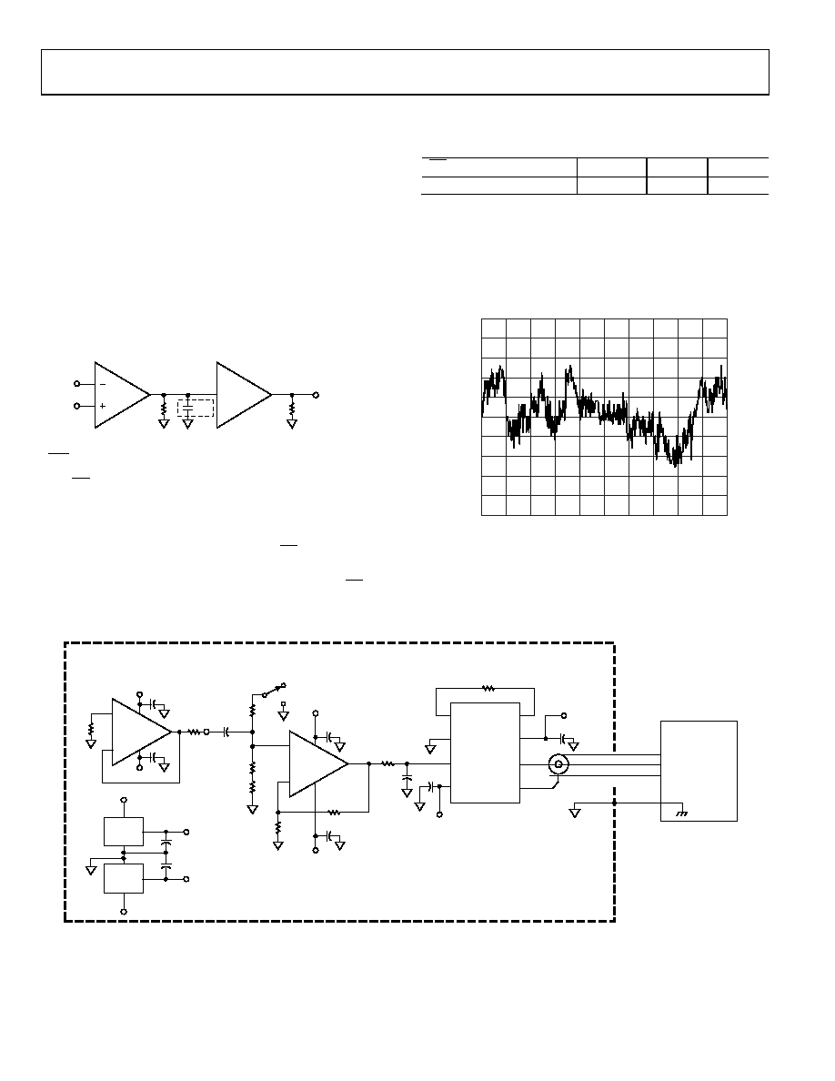
0.1 Hz TO 10 Hz NOISE
Figure 45 shows the 0.1 Hz to 10 Hz voltage and current noise
of the ADA4898. The peak-to-peak noise voltage is below 0.5 μV.
Figure 46 shows the circuit used to measure the low frequency
noise. It uses a band-pass filter of approximately 0.1 Hz and 10 Hz
and a high gain stage feeding into an instrumentation amplifier.
0.5
0.4
0.3
0.2
0.1
0
–0.1
–0.2
–0.3
–0.4
–0.5
02
4
6
8
10
12
14
16
18
20
TIME (s)
O
U
T
PU
T
VO
L
T
A
G
E
(
V
)
07
03
7-
0
47
Figure 45. 0.1 Hz to 10 Hz Noise
DUT
ADA4898-1
+IN
–IN
1F
10nF
50
+IN
–IN
AD743
–VS = –9V
+VS = +9V
1F
15.8k
13k
13
MOMENTARY
1k
806k
7805
7905
+VS = +9V
(BATTERY)
–VS = –9V
(BATTERY)
+VR = +5V
–VR = –5V
+VR = +5V
–VR = –5V
AD620
RG
–IN
+IN
–VS
RG
+VS
OUTPUT
REF
R = 5.36k, GAIN APPROX. 10
10nF
1
2
4
3
8
7
5
6
10nF
+VS = +9V
–VS = –9V
FLOATING SHIELD
COAX
TEK
TDS 754A SCOPE
IN
FARADAY CAGE
07
037
-04
8
OUT
Figure 46. Low Frequency Noise Circuit
相关PDF资料 |
PDF描述 |
|---|---|
| TSW-136-14-S-D | CONN HEADER 72POS .100" DL GOLD |
| 951110-7722-AR | CONN HEADER 10POS 2MM R/A SOLDER |
| PBC33DBDN | CONN HEADER .100 DUAL R/A 66POS |
| 77313-118-18LF | BERGSTIK |
| 0234008.MXP | FUSE NORM 250VAC 8A 5X20 |
相关代理商/技术参数 |
参数描述 |
|---|---|
| ADA4899 | 制造商:AD 制造商全称:Analog Devices 功能描述:Dual-Current Output, Parallel Input, 16 /14-Bit Multiplying DACs with 4-Quadrant Resistors |
| ADA4899-1 | 制造商:AD 制造商全称:Analog Devices 功能描述:1 nV/√Hz, Low Power, Rail-to-Rail Output Amplifiers |
| ADA4899-1_07 | 制造商:AD 制造商全称:Analog Devices 功能描述:Unity-Gain Stable, Ultralow Distortion, 1 nV/☆Hz Voltage Noise, High Speed Op Amp |
| ADA4899-1YCP-EBZ | 功能描述:BOARD EVAL FOR ADA4899-1YCP RoHS:是 类别:编程器,开发系统 >> 评估板 - 运算放大器 系列:- 产品培训模块:Lead (SnPb) Finish for COTS Obsolescence Mitigation Program 标准包装:1 系列:- |
| ADA4899-1YCPZ-R2 | 制造商:Analog Devices 功能描述:OP Amp Single Volt Fdbk ±6V/12V 8-Pin LFCSP EP T/R 制造商:Analog Devices 功能描述:OP AMP SGL VOLT FDBK 6V/12V 8LFCSP - Tape and Reel 制造商:Rochester Electronics LLC 功能描述:ULTRA LOW NOISE AND DISTORTION HI SPEED - Bulk 制造商:Analog Devices 功能描述:IC OP-AMP 600MHZ 310V/ LFCSP-8 制造商:Analog Devices 功能描述:IC, OP-AMP, 600MHZ, 310V/s, LFCSP-8, Op Amp Type:Voltage Feedback, No. of Ampli |
发布紧急采购,3分钟左右您将得到回复。