- 您现在的位置:买卖IC网 > PDF目录2139 > ADA4899-1YRDZ-R7 (Analog Devices Inc)IC OPAMP VF ULN ULDIST 8SOIC PDF资料下载
参数资料
| 型号: | ADA4899-1YRDZ-R7 |
| 厂商: | Analog Devices Inc |
| 文件页数: | 6/21页 |
| 文件大小: | 0K |
| 描述: | IC OPAMP VF ULN ULDIST 8SOIC |
| 产品培训模块: | Practical Guide High Speed PCB Layout |
| 设计资源: | High Speed, Precision, Differential AC-Coupled Drive Circuit for AD7625 (CN0080) |
| 标准包装: | 1,000 |
| 放大器类型: | 电压反馈 |
| 电路数: | 1 |
| 转换速率: | 310 V/µs |
| -3db带宽: | 600MHz |
| 电流 - 输入偏压: | 6µA |
| 电压 - 输入偏移: | 35µV |
| 电流 - 电源: | 14.7mA |
| 电流 - 输出 / 通道: | 200mA |
| 电压 - 电源,单路/双路(±): | 4.5 V ~ 12 V,±2.25 V ~ 6 V |
| 工作温度: | -40°C ~ 125°C |
| 安装类型: | 表面贴装 |
| 封装/外壳: | 8-SOIC(0.154",3.90mm Width)裸露焊盘 |
| 供应商设备封装: | 8-SOIC-EP |
| 包装: | 带卷 (TR) |
ADA4899-1
Rev. B | Page 13 of 20
THEORY OF OPERATION
The ADA4899-1 is a voltage feedback op amp that combines
unity-gain stability with a 1 nV/√Hz input noise. It employs a
highly linear input stage that can maintain greater than 80 dBc
(@ 2 V p-p) distortion out to 10 MHz while in a unity-gain
configuration. This rare combination of low gain stability,
input-referred noise, and extremely low distortion is the result
of Analog Devices proprietary op amp architecture and high
speed complementary bipolar processing technology.
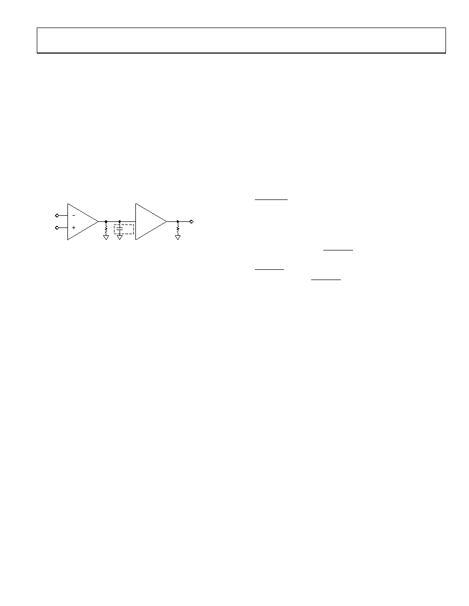
The simplified ADA4899-1 topology, shown in Figure 45, is a
single gain stage with a unity-gain output buffer. It has over
80 dB of open-loop gain and maintains precision specifications
such as CMRR, PSRR, and offset to levels that are normally
associated with topologies having two or more gain stages.
BUFFER
gm
CC
R1
RL
VOUT
0
5
72
0
-06
0
Figure 45. ADA4899-1 Topology
A pair of internally connected diodes limits the differential
voltage between the noninverting input and the inverting input
of the ADA4899-1. Each set of diodes has two series diodes
connected in antiparallel, which limits the differential voltage
between the inputs to approximately ±1.2 V. All of the ADA4899-1
pins are ESD protected with voltage-limiting diodes connected
between both rails. The protection diodes can handle 10 mA.
Currents should be limited through these diodes to 10 mA or less
by using a series limiting resistor.
PACKAGING INNOVATION
The ADA4899-1 is available in both a SOIC and an LFCSP, each
of which has a thermal pad that allows the device to run cooler,
thereby increasing reliability. To help avoid routing around the
pad when laying out the board, both packages have a dedicated
feedback pin on the opposite side of the package for ease in
connecting the feedback network to the inverting input. The
secondary output pin also isolates the interaction of any
capacitive load on the output and the self-inductance of the
package and bond wire from the feedback loop. When using the
dedicated feedback pin, inductance in the primary output helps to
isolate capacitive loads from the output impedance of the
amplifier.
Both the SOIC and LFCSP have modified pinouts to improve
heavy load second harmonic distortion performance. The intent
of both is to isolate the negative supply pin from the noninverting
input. The LFCSP accomplishes this by rotating the standard
8-lead package pinout counterclockwise by one pin, which puts
the supply and output pins on the right side of the package and
the input pins on the left side of the package. The SOIC is
slightly different with the intent of both isolating the inputs
from the supply pins and giving the user the option of using the
ADA4899-1 in a standard SOIC board layout with little or no
modification. Taking the unused Pin 5 and making it a second
negative supply pin allows for both an input isolated layout and
a traditional layout to be supported.
DISABLE PIN
A three-state input pin is provided on the ADA4899-1 for a
high impedance disable and an optional input bias current
cancellation circuit. The high impedance output allows several
ADA4899-1s to drive the same ADC or output line time
interleaved. Pulling the DISABLE pin low activates the high
impedance state (see Table 7 for threshold levels). When the
DISABLE pin is left floating (open), the ADA4899-1 operates
normally. With the DISABLE pin pulled within 0.7 V of the
positive supply, an optional input bias current cancellation
circuit is turned on, which lowers the input bias current to less
than 200 nA. In this mode, the user can drive the ADA4899-1
from a high dc source impedance and still maintain minimal
output-referred offset without having to use impedance
matching techniques. In addition, the ADA4899-1 can be
ac-coupled while setting the bias point on the input with a high
dc impedance network. The input bias current cancellation
circuit doubles the input-referred current noise, but this effect is
minimal as long as the wideband impedances are kept low (see
相关PDF资料 |
PDF描述 |
|---|---|
| ADA4927-2YCPZ-R2 | IC OPAMP CF DIFF DUAL LN 24LFCSP |
| ADA4930-1YCPZ-R2 | IC DIFF AMP 1.35GHZ 16-LFCSP |
| ADA4932-1YCPZ-RL | IC AMP DIFF LP 80MA 16LFCSP |
| ADA4939-2YCPZ-R7 | IC AMP DIFF DUAL ULDIST 24LFCSP |
| ADA4940-1ARZ-R7 | IC DIFF ADC DVR 18BIT LN 8SOIC |
相关代理商/技术参数 |
参数描述 |
|---|---|
| ADA4899-1YRDZ-RL | 功能描述:IC OPAMP VF ULN ULDIST 8SOIC RoHS:是 类别:集成电路 (IC) >> Linear - Amplifiers - Instrumentation 系列:- 标准包装:50 系列:LinCMOS™ 放大器类型:通用 电路数:4 输出类型:- 转换速率:0.05 V/µs 增益带宽积:110kHz -3db带宽:- 电流 - 输入偏压:0.7pA 电压 - 输入偏移:210µV 电流 - 电源:57µA 电流 - 输出 / 通道:30mA 电压 - 电源,单路/双路(±):3 V ~ 16 V,±1.5 V ~ 8 V 工作温度:-40°C ~ 85°C 安装类型:表面贴装 封装/外壳:14-SOIC(0.154",3.90mm 宽) 供应商设备封装:14-SOIC 包装:管件 产品目录页面:865 (CN2011-ZH PDF) 其它名称:296-1834296-1834-5 |
| ADA4922-1 | 制造商:AD 制造商全称:Analog Devices 功能描述:14-Bit, 1 MSPS, Differential, Programmable Input PulSAR ADC |
| ADA4922-1ACP-EBZ | 功能描述:BOARD EVAL FOR ADA4922-1ACP RoHS:是 类别:编程器,开发系统 >> 评估板 - 运算放大器 系列:- 产品培训模块:Lead (SnPb) Finish for COTS Obsolescence Mitigation Program 标准包装:1 系列:- |
| ADA4922-1ACPZ-R2 | 功能描述:IC ADC DRIVER 18BIT DIFF 8-LFCSP RoHS:是 类别:集成电路 (IC) >> 线性 - 放大器 - 专用 系列:- 产品培训模块:Lead (SnPb) Finish for COTS Obsolescence Mitigation Program 标准包装:60 系列:- 类型:可变增益放大器 应用:CATV 安装类型:表面贴装 封装/外壳:20-WQFN 裸露焊盘 供应商设备封装:20-TQFN-EP(5x5) 包装:托盘 |
| ADA4922-1ACPZ-R7 | 制造商:Analog Devices 功能描述:SP AMP DIFF LINE DRVR AMP SGL R-R O/P 26V 8LFCSP EP - Bulk |
发布紧急采购,3分钟左右您将得到回复。