- 您现在的位置:买卖IC网 > PDF目录2063 > ADA4922-1ACPZ-R2 (Analog Devices Inc)IC ADC DRIVER 18BIT DIFF 8-LFCSP PDF资料下载
参数资料
| 型号: | ADA4922-1ACPZ-R2 |
| 厂商: | Analog Devices Inc |
| 文件页数: | 9/20页 |
| 文件大小: | 0K |
| 描述: | IC ADC DRIVER 18BIT DIFF 8-LFCSP |
| 标准包装: | 1 |
| 类型: | ADC 驱动器 |
| 应用: | 数据采集 |
| 安装类型: | 表面贴装 |
| 封装/外壳: | 8-VFDFN 裸露焊盘,CSP |
| 供应商设备封装: | 8-LFCSP-VD(3x3) |
| 包装: | 标准包装 |
| 其它名称: | ADA4922-1ACPZ-R2DKR |
ADA4922-1
Rev. 0 | Page 17 of 20
Defining VIN as the voltage applied to the input pin, the
equations that govern the two signal paths are given in
Equation 12 and Equation 13.
VOUT+ = +VIN
(12)
VOUT = VIN + 2(REF)
(13)
When the REF voltage is set to the midswing level of the input
signal, the two output signals fall directly on top of each other
with minimal offset. Setting the REF voltage elsewhere results
in an offset between the two outputs. This effect is illustrated in
the Theory of Operation section.
The best use of the REF pin can be further illustrated by
considering a single-supply example that uses a 10 V dc power
supply and has an input signal that varies between 2 V and 7 V.
This is a case where the midswing level of the input signal is not
at midsupply but is at 4.5 V. By setting the REF input to 4.5 V
and neglecting offsets, Equation 12 and Equation 13 are used to
calculate the results. When the input signal is at its midpoint of
4.5 V, VOUT+ is at 4.5 V, as is VOUT. This can be considered as a
type of baseline state where the differential output voltage is
zero. When the input increases to 7 V, VOUT+ tracks the input to
7 V and VOUT decreases to 2 V. This can be viewed as a positive
peak signal where the differential output voltage equals 5 V.
When the input signal decreases to 2 V, VOUT+ again tracks to
2 V, and VOUT increases to 7 V. This can be viewed as a negative
peak signal where the differential output voltage equals 5 V.
The resulting differential output voltage is 10 V p-p.
The previous discussion exposes how the single-ended-to-
differential gain of 2 is achieved.
INTERNAL FEEDBACK NETWORK POWER
DISSIPATION
While traditional op amps do not have on-chip feedback
elements, the ADA4922-1 contains two on-chip 600 Ω resistors
that comprise an internal feedback loop. The power dissipated
in these resistors must be included in the overall power dissipation
calculations for the device. Under certain circumstances, the
power dissipated in these resistors could be considerably more
than the device’s quiescent current. For example, on ±12 V
supplies with the REF pin tied to ground and OUT at 9 V dc,
each 600 Ω resistor carries 15 mA and dissipates 135 mW. This
is a significant amount of power and must therefore be included
in the overall device power dissipation calculations. For ac
signals, rms analysis is required.
DISABLE FEATURE
The ADA4922-1 includes a disable feature that can be asserted
to minimize power consumption in a device that is not needed
at a particular time. When asserted, the disable feature does not
place the device output in a high impedance or three-state
condition. The disable feature is asserted by applying a control
voltage to the DIS pin and is active low. See the Specifications
section for the high and low level voltage specifications.
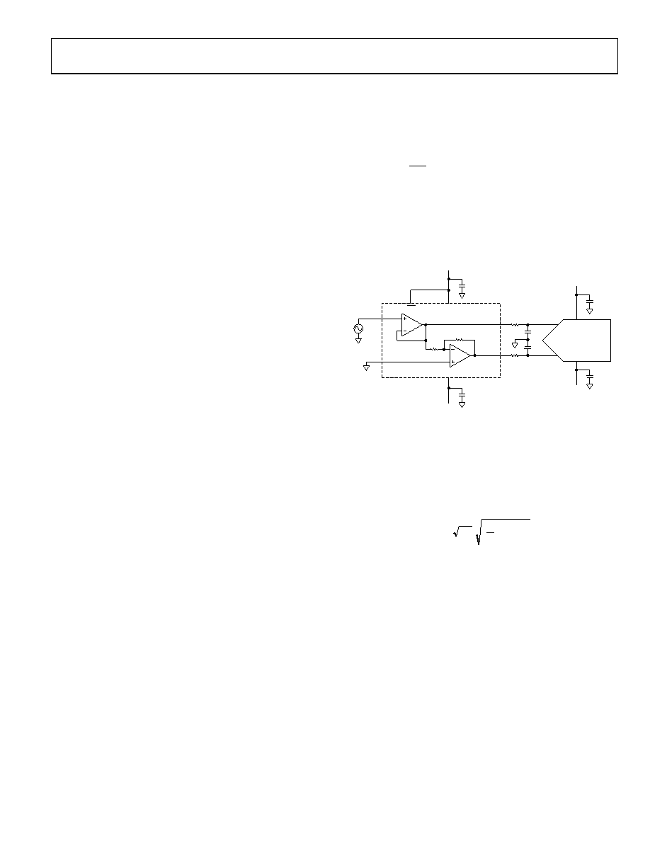
DRIVING A DIFFERENTIAL INPUT ADC
The ADA4922-1 provides the single-ended-to-differential
conversion that is required to drive most high resolution ADCs.
Figure 50 shows how the ADA4922-1 simplifies ADC driving.
VIN
±10V
0.1
μF
–12V
HIGH VOLTAGE
HIGH RESOLUTION
ADC
VS–
VS+
DIS
056
81
-0
49
R
IN
8
OUT+
ADA4922-1
OUT–
4
5
6
73
REF
2
0.1
μF
–12V
0.1
μF
+12V
0.1
μF
+12V
R
C
Figure 50. Driving a Differential Input ADC
For example, consider the case where the input signal
bandwidth is 100 KHz and R = 41.2 Ω and C = 3.9 nF, as is
shown in Figure 50, to form a single-pole filter with 3 dB
bandwidth of approximately 1 MHz. The ADA4922-1 output
noise (with zero source resistance) integrated over this
bandwidth appears at the ADC input and is calculated as
()
rms
μV
15
MHz
1
2
π
Hz
nV/
12
)
(
,
=
=
rms
V
dm
ADC
n,
(14)
The rms value of a 20 V p-p signal at the ADC input is 7 V rms,
yielding a SNR of 113 dB at the ADC input.
相关PDF资料 |
PDF描述 |
|---|---|
| ADA4937-2YCPZ-RL | IC ADC DRIVER DUAL DIFF 24LFCSP |
| ADA4938-2ACPZ-RL | IC ADC DRIVER DUAL DIFF 24LFCSP |
| ADA4941-1YRZ-R7 | IC DIFF ADC DRIVER 18BIT 8SOIC |
| ADA4960-1ACPZ-R2 | IC ADC DRIVER DIFF 16LFCSP |
| ADATE205BSVZ | IC DCL DUAL 250MHZ ATE 100TQFP |
相关代理商/技术参数 |
参数描述 |
|---|---|
| ADA4922-1ACPZ-R7 | 制造商:Analog Devices 功能描述:SP AMP DIFF LINE DRVR AMP SGL R-R O/P 26V 8LFCSP EP - Bulk |
| ADA4922-1ACPZ-RL | 功能描述:IC ADC DRIVER 18BIT DIFF 8-LFCSP RoHS:是 类别:集成电路 (IC) >> 线性 - 放大器 - 专用 系列:- 产品培训模块:Lead (SnPb) Finish for COTS Obsolescence Mitigation Program 标准包装:60 系列:- 类型:可变增益放大器 应用:CATV 安装类型:表面贴装 封装/外壳:20-WQFN 裸露焊盘 供应商设备封装:20-TQFN-EP(5x5) 包装:托盘 |
| ADA4922-1ACPZ-RL7 | 功能描述:IC ADC DRVR 18BIT HV DIFF 8LFCSP RoHS:是 类别:集成电路 (IC) >> 线性 - 放大器 - 专用 系列:- 产品培训模块:Lead (SnPb) Finish for COTS Obsolescence Mitigation Program 标准包装:60 系列:- 类型:可变增益放大器 应用:CATV 安装类型:表面贴装 封装/外壳:20-WQFN 裸露焊盘 供应商设备封装:20-TQFN-EP(5x5) 包装:托盘 |
| ADA4922-1ARD-EBZ | 功能描述:BOARD EVAL FOR ADA4922-1ARD RoHS:是 类别:编程器,开发系统 >> 评估板 - 运算放大器 系列:- 产品培训模块:Lead (SnPb) Finish for COTS Obsolescence Mitigation Program 标准包装:1 系列:- |
| ADA4922-1ARDZ | 功能描述:IC ADC DRVR 18BIT HV DIFF 8-SOIC RoHS:是 类别:集成电路 (IC) >> 线性 - 放大器 - 专用 系列:- 产品培训模块:Lead (SnPb) Finish for COTS Obsolescence Mitigation Program 标准包装:60 系列:- 类型:可变增益放大器 应用:CATV 安装类型:表面贴装 封装/外壳:20-WQFN 裸露焊盘 供应商设备封装:20-TQFN-EP(5x5) 包装:托盘 |
发布紧急采购,3分钟左右您将得到回复。