- 您现在的位置:买卖IC网 > PDF目录16959 > ADA4927-1YCP-EBZ (Analog Devices Inc)BOARD EVAL FOR ADA4927-1YCP PDF资料下载
参数资料
| 型号: | ADA4927-1YCP-EBZ |
| 厂商: | Analog Devices Inc |
| 文件页数: | 15/24页 |
| 文件大小: | 0K |
| 描述: | BOARD EVAL FOR ADA4927-1YCP |
| 标准包装: | 1 |
| 每 IC 通道数: | 1 - 单 |
| 放大器类型: | 差分 |
| 板类型: | 裸(未填充) |
| 已供物品: | 板 |
| 已用 IC / 零件: | 16-LFCSP 封装 |
ADA4927-1/ADA4927-2
Rev. A | Page 22 of 24
LAYOUT, GROUNDING, AND BYPASSING
As a high speed device, the ADA4927 is sensitive to the PCB
environment in which it operates. Realizing its superior performance
requires attention to the details of high speed PCB design. This
section shows a detailed example of how the ADA4927-1 was
addressed.
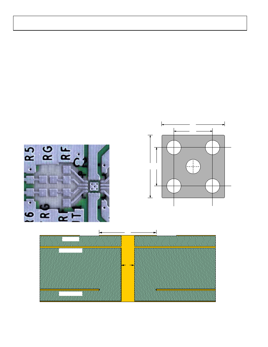
The first requirement is a solid ground plane that covers as
much of the board area around the ADA4927-1 as possible.
However, clear the area near the feedback resistors (RF), gain
resistors (RG), and the input summing nodes (Pin 2 and Pin 3) of
all ground and power planes (see Figure 55). Clearing the ground
and power planes minimizes any stray capacitance at these nodes
and prevents peaking of the response of the amplifier at high
frequencies. Whereas ideal current feedback amplifiers are
insensitive to summing node capacitance, real-world amplifiers
can exhibit peaking due to excessive summing node capacitance.
The thermal resistance, θJA, is specified for the device, including
the exposed pad, soldered to a high thermal conductivity 4-layer
circuit board, as described in EIA/JESD 51-7.
0
75
74
-0
55
Figure 55. Ground and Power Plane Voiding in Vicinity of RF AND RG
Bypassed the power supply pins as close to the device as possible
and directly to a nearby ground plane. Use high frequency ceramic
chip capacitors. It is recommended that two parallel bypass
capacitors (1000 pF and 0.1 μF) be used for each supply. The
1000 pF capacitor should be placed closer to the device. Further
away, provide low frequency bulk bypassing, using 10 μF
tantalum capacitors from each supply to ground.
Make signal routing short and direct to avoid parasitic effects.
Wherever complementary signals exist, provide a symmetrical
layout to maximize balanced performance. When routing
differential signals over a long distance, place PCB traces close
together, and twist any differential wiring such that the loop
area is minimized. Doing this reduces radiated energy and
makes the circuit less susceptible to interference.
1.30
0.80
1.30
07
57
4-
0
56
Figure 56. Recommended PCB Thermal Attach Pad Dimensions (Millimeters)
1.30
0.30
PLATED
VIA HOLE
GROUND PLANE
POWER PLANE
BOTTOM METAL
TOP METAL
4-
05
7
07
57
Figure 57. Cross-Section of 4-Layer PCB Showing Thermal Via Connection to Buried Ground Plane (Dimensions in Millimeters)
相关PDF资料 |
PDF描述 |
|---|---|
| ECM12DRTI-S13 | CONN EDGECARD 24POS .156 EXTEND |
| 1-1589476-0 | CONN RCPT 15POS 28AWG 3M |
| ECM12DRKI-S13 | CONN EDGECARD 24POS .156 EXTEND |
| VE-JTL-EY | CONVERTER MOD DC/DC 28V 50W |
| ADA4851-4YRU-EBZ | BOARD EVAL FOR ADA4851-4YRU |
相关代理商/技术参数 |
参数描述 |
|---|---|
| ADA4927-1YCPZ-R2 | 制造商:Analog Devices 功能描述:SP Amp Differential ADC Driver Single 11V 16-Pin LFCSP EP T/R 制造商:Analog Devices 功能描述:SP AMP DIFFERENTIAL ADC DRVR SGL 11V 16LFCSP EP - Tape and Reel 制造商:Analog Devices 功能描述:ANAADA4927-1YCPZ-R2 ULTRALW DISTORTION C 制造商:Analog Devices 功能描述:OP AMP CF DIFF 65MA LN 16LFCSP 制造商:Analog Devices 功能描述:OP AMP, CF, DIFF, 65MA, LN, 16LFCSP 制造商:Analog Devices 功能描述:OP AMP, CF, DIFF, 65MA, LN, 16LFCSP; No. of Amplifiers:1; Input Offset Voltage:1.3mV; Bandwidth:2.3GHz; Amplifier Case Style:LFCSP; No. of Pins:16; Supply Voltage Range:4.5V to 11V; Slew Rate:5000V/s; Supply Current:20mA; Operating ;RoHS Compliant: Yes |
| ADA4927-1YCPZ-R2 | 制造商:Analog Devices 功能描述:IC DIFF AMP 2.3GHZ 5000V/ LFCSP-16 |
| ADA4927-1YCPZ-R7 | 功能描述:IC OPAMP CF DIFF 65MA LN 16LFCSP RoHS:是 类别:集成电路 (IC) >> Linear - Amplifiers - Instrumentation 系列:- 标准包装:2,500 系列:- 放大器类型:通用 电路数:4 输出类型:- 转换速率:0.6 V/µs 增益带宽积:1MHz -3db带宽:- 电流 - 输入偏压:45nA 电压 - 输入偏移:2000µV 电流 - 电源:1.4mA 电流 - 输出 / 通道:40mA 电压 - 电源,单路/双路(±):3 V ~ 32 V,±1.5 V ~ 16 V 工作温度:0°C ~ 70°C 安装类型:表面贴装 封装/外壳:14-TSSOP(0.173",4.40mm 宽) 供应商设备封装:14-TSSOP 包装:带卷 (TR) 其它名称:LM324ADTBR2G-NDLM324ADTBR2GOSTR |
| ADA4927-1YCPZ-RL | 功能描述:IC OPAMP CF DIFF 65MA LN 16LFCSP RoHS:是 类别:集成电路 (IC) >> Linear - Amplifiers - Instrumentation 系列:- 标准包装:50 系列:- 放大器类型:J-FET 电路数:2 输出类型:- 转换速率:13 V/µs 增益带宽积:3MHz -3db带宽:- 电流 - 输入偏压:65pA 电压 - 输入偏移:3000µV 电流 - 电源:1.4mA 电流 - 输出 / 通道:- 电压 - 电源,单路/双路(±):7 V ~ 36 V,±3.5 V ~ 18 V 工作温度:-40°C ~ 85°C 安装类型:通孔 封装/外壳:8-DIP(0.300",7.62mm) 供应商设备封装:8-PDIP 包装:管件 |
| ADA4927-2 | 制造商:AD 制造商全称:Analog Devices 功能描述:Ultralow Distortion Current Feedback Differential ADC Driver |
发布紧急采购,3分钟左右您将得到回复。