- 您现在的位置:买卖IC网 > PDF目录16928 > ADA4927-2YCP-EBZ (Analog Devices Inc)BOARD EVAL FOR ADA4927-2YCP PDF资料下载
参数资料
| 型号: | ADA4927-2YCP-EBZ |
| 厂商: | Analog Devices Inc |
| 文件页数: | 11/24页 |
| 文件大小: | 0K |
| 描述: | BOARD EVAL FOR ADA4927-2YCP |
| 标准包装: | 1 |
| 每 IC 通道数: | 2 - 双 |
| 放大器类型: | 差分 |
| 板类型: | 裸(未填充) |
| 已供物品: | 板 |
| 已用 IC / 零件: | 24-LFCSP 封装 |
ADA4927-1/ADA4927-2
Rev. A | Page 19 of 24
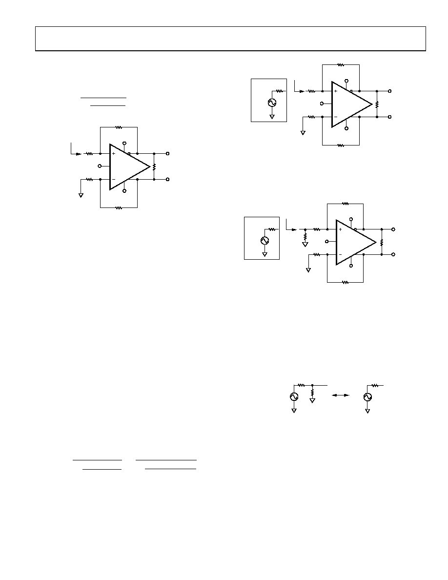
For an unbalanced, single-ended input signal (see Figure 49),
the input impedance is
()
+
×
=
F
G
F
G
SE
IN
R
2
1
,
ADA4927
RL VOUT, dm
+VS
–VS
RG
RF
VOCM
RIN, SE
0
75
74
-04
9
Figure 49. The ADA4927 with Unbalanced (Single-Ended) Input
The input impedance of the circuit is effectively higher than it
would be for a conventional op amp connected as an inverter
because a fraction of the differential output voltage appears at
the inputs as a common-mode signal, partially bootstrapping
the voltage across the input resistor RG. The common-mode
voltage at the amplifier input terminals can be easily determined
by noting that the voltage at the inverting input is equal to the
noninverting output voltage divided down by the voltage divider
formed by RF and RG in the lower loop. This voltage is present at
both input terminals due to negative voltage feedback and is in
phase with the input signal, thus reducing the effective voltage
across RG in the upper loop and partially bootstrapping RG.
Terminating a Single-Ended Input
This section deals with how to properly terminate a single-
ended input to the ADA4927 with a gain of 1, RF = 348 Ω, and
RG = 348 Ω. An example using an input source with a terminated
output voltage of 1 V p-p and a source resistance of 50 Ω illustrates
the four simple steps that must be followed. Note that, because
the terminated output voltage of the source is 1 V p-p, the open
circuit output voltage of the source is 2 V p-p. The source shown
in Figure 50 indicates this open-circuit voltage.
1. The input impedance must be calculated using the following
formula:
464
)
348
(
2
348
1
348
)
(
2
1
=
+
×
=
+
×
=
F
G
F
G
IN
R
RS
50
VS
2V p-p
RIN
464
ADA4927
RL VOUT, dm
+VS
–VS
RF
348
RG
348
RG
348
VOCM
RF
348
07
57
4-
0
50
Figure 50. Calculating Single-Ended Input Impedance RIN
2.
To match the 50 Ω source resistance, the termination
resistor, RT, is calculated using RT||464 Ω = 50 Ω. The
closest standard 1% value for RT is 56.2 Ω.
ADA4927
RL
VOUT, dm
+VS
–VS
RF
348
RS
50
VS
2V p-p
RIN
50
RG
348
RG
348
RT
56.2
VOCM
RF
348
0
757
4-
05
1
Figure 51. Adding Termination Resistor RT
3.
upper feedback loop is now greater than the RG in the
lower loop due to the addition of the termination resistors.
To compensate for the imbalance of the gain resistors,
a correction resistor (RTS) is added in series with RG in the
lower loop. RTS is equal to the Thevenin equivalent of the
source resistance RS and the termination resistance RT and
is equal to RS||RT.
RS
50
VS
2V p-p
RTH
26.5
RT
56.2
VTH
1.06V p-p
0
75
74
-05
2
Figure 52. Calculating the Thevenin Equivalent
相关PDF资料 |
PDF描述 |
|---|---|
| ADA4922-1ARD-EBZ | BOARD EVAL FOR ADA4922-1ARD |
| VI-24M-EY | CONVERTER MOD DC/DC 10V 50W |
| 512452-000 | BOOT MOLDED |
| 3-1589476-5 | CONN RCPT 51POS 30AWG 24IN |
| ESM10DTKI-S288 | CONN EDGECARD 20POS .156 EXTEND |
相关代理商/技术参数 |
参数描述 |
|---|---|
| ADA4927-2YCPZ-R2 | 功能描述:IC OPAMP CF DIFF DUAL LN 24LFCSP RoHS:是 类别:集成电路 (IC) >> Linear - Amplifiers - Instrumentation 系列:- 标准包装:1,000 系列:- 放大器类型:电压反馈 电路数:4 输出类型:满摆幅 转换速率:33 V/µs 增益带宽积:20MHz -3db带宽:30MHz 电流 - 输入偏压:2nA 电压 - 输入偏移:3000µV 电流 - 电源:2.5mA 电流 - 输出 / 通道:30mA 电压 - 电源,单路/双路(±):4.5 V ~ 16.5 V,±2.25 V ~ 8.25 V 工作温度:-40°C ~ 85°C 安装类型:表面贴装 封装/外壳:14-SOIC(0.154",3.90mm 宽) 供应商设备封装:14-SOIC 包装:带卷 (TR) |
| ADA4927-2YCPZ-R7 | 功能描述:IC OPAMP CF DIFF DUAL LN 24LFCSP RoHS:是 类别:集成电路 (IC) >> Linear - Amplifiers - Instrumentation 系列:- 标准包装:2,500 系列:Excalibur™ 放大器类型:J-FET 电路数:1 输出类型:- 转换速率:45 V/µs 增益带宽积:10MHz -3db带宽:- 电流 - 输入偏压:20pA 电压 - 输入偏移:490µV 电流 - 电源:1.7mA 电流 - 输出 / 通道:48mA 电压 - 电源,单路/双路(±):4.5 V ~ 38 V,±2.25 V ~ 19 V 工作温度:-40°C ~ 85°C 安装类型:表面贴装 封装/外壳:8-SOIC(0.154",3.90mm 宽) 供应商设备封装:8-SOIC 包装:带卷 (TR) |
| ADA4927-2YCPZ-RL | 功能描述:IC OPAMP CF DIFF DUAL LN 24LFCSP RoHS:是 类别:集成电路 (IC) >> Linear - Amplifiers - Instrumentation 系列:- 标准包装:2,500 系列:Excalibur™ 放大器类型:J-FET 电路数:1 输出类型:- 转换速率:45 V/µs 增益带宽积:10MHz -3db带宽:- 电流 - 输入偏压:20pA 电压 - 输入偏移:490µV 电流 - 电源:1.7mA 电流 - 输出 / 通道:48mA 电压 - 电源,单路/双路(±):4.5 V ~ 38 V,±2.25 V ~ 19 V 工作温度:-40°C ~ 85°C 安装类型:表面贴装 封装/外壳:8-SOIC(0.154",3.90mm 宽) 供应商设备封装:8-SOIC 包装:带卷 (TR) |
| ADA4930-1 | 制造商:AD 制造商全称:Analog Devices 功能描述:Ultralow Noise Drivers for Low Voltage ADCs |
| ADA4930-1SCPZ-EPR2 | 制造商:Analog Devices 功能描述:ULTRALOW DIST LOW VLTG ADC DRIVER - Tape and Reel 制造商:Analog Devices 功能描述:Differential Amplifiers UltraLow Dist Low Vltg ADC Driver |
发布紧急采购,3分钟左右您将得到回复。