- 您现在的位置:买卖IC网 > PDF目录16955 > ADA4930-1YCP-EBZ (Analog Devices Inc)BOARD EVAL FOR ADA4930-1YCP PDF资料下载
参数资料
| 型号: | ADA4930-1YCP-EBZ |
| 厂商: | Analog Devices Inc |
| 文件页数: | 17/29页 |
| 文件大小: | 0K |
| 描述: | BOARD EVAL FOR ADA4930-1YCP |
| 标准包装: | 1 |
| 每 IC 通道数: | 1 - 单 |
| 放大器类型: | 差分 |
| 板类型: | 裸(未填充) |
| 已供物品: | 板 |
| 已用 IC / 零件: | 16-LFCSP 封装 |
第1页第2页第3页第4页第5页第6页第7页第8页第9页第10页第11页第12页第13页第14页第15页第16页当前第17页第18页第19页第20页第21页第22页第23页第24页第25页第26页第27页第28页第29页
ADA4930-1/ADA4930-2
Rev. A | Page 23 of 28
LAYOUT, GROUNDING, AND BYPASSING
The ADA4930-1/ADA4930-2 are high speed devices. Realizing
their superior performance requires attention to the details of
high speed PCB design.
The first requirement is to use a multilayer PCB with solid ground
and power planes that cover as much of the board area as possible.
Bypass each power supply pin directly to a nearby ground plane, as
close to the device as possible. Use 0.1 μF high frequency ceramic
chip capacitors.
Provide low frequency bulk bypassing, using 10 μF tantalum
capacitors from each supply to ground.
Stray transmission line capacitance in combination with package
parasitics can potentially form a resonant circuit at high frequencies,
resulting in excessive gain peaking or possible oscillation.
Signal routing should be short and direct to avoid such parasitic
effects. Provide symmetrical layout for complementary signals
to maximize balanced performance.
0
92
09
-0
58
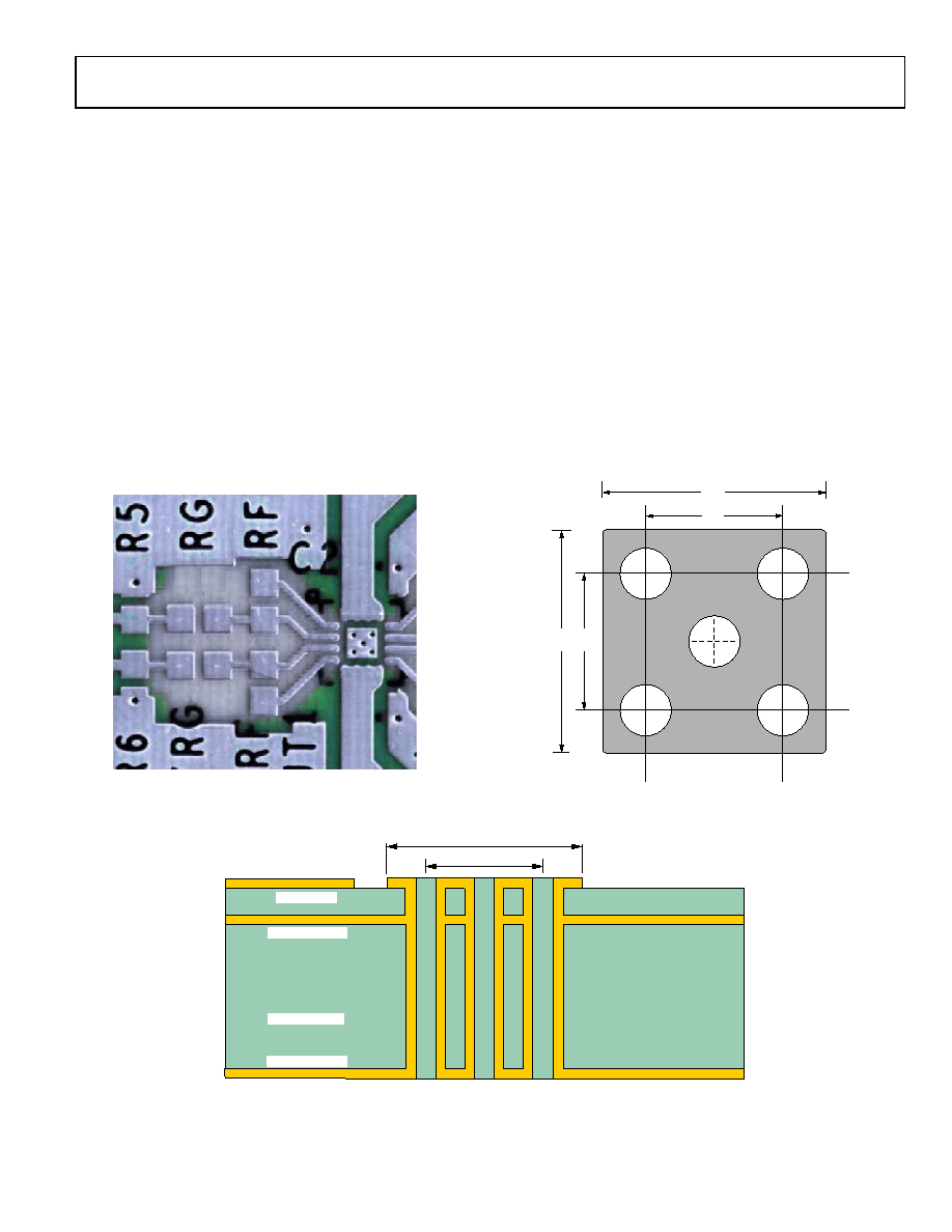
Figure 56. ADA4930-1 Ground and Power Plane Voiding
in the Vicinity of RF and RG
Use radio frequency transmission lines to connect the driver
and receiver to the amplifier.
Minimize stray capacitance at the input/output pins by clearing
the underlying ground and low impedance planes near these pins
If the driver/receiver is more than one-eighth of the wavelength
from the amplifier, the signal trace widths should be minimal.
This nontransmission line configuration requires the underlying
and adjacent ground and low impedance planes to be cleared
near the signal lines.
The exposed thermal paddle is internally connected to the ground
pin of the amplifier. Solder the paddle to the low impedance
ground plane on the PCB to ensure the specified electrical
performance and to provide thermal relief. To reduce thermal
impedance further, it is recommended that the ground planes
on all layers under the paddle be connected together with vias.
1.30
0.80
1.30
09
20
9-
0
59
Figure 57. Recommended PCB Thermal Attach Pad Dimensions (Millimeters)
0.8 mm
1.3 mm
POWER PLANE
GROUND PLANE
TOP METAL
BOTTOM METAL
09
20
9-
06
0
Figure 58. Cross-Section of 4-Layer PCB Showing Thermal Via Connection to Buried Ground Plane (Dimensions in Millimeters)
相关PDF资料 |
PDF描述 |
|---|---|
| ECM18DRTI-S13 | CONN EDGECARD 36POS .156 EXTEND |
| 7-1589455-2 | WDUALOBE CONNECTOR |
| SRR0905-270M | INDUCTOR POWER 27UH 1.3A SMD |
| SP1210R-124K | INDUCTOR PWR SHIELDED 120UH SMD |
| 202D221-25/86-0 | BOOT MOLDED |
相关代理商/技术参数 |
参数描述 |
|---|---|
| ADA4930-1YCPZ | 制造商:Analog Devices 功能描述:IC AMP DIFF 1.35GHZ 16-LFCSP 制造商:Analog Devices 功能描述:IC, AMP, DIFF, 1.35GHZ, 16-LFCSP 制造商:Analog Devices 功能描述:IC, AMP, DIFF, 1.35GHZ, 16-LFCSP; No. of Amplifiers:1; Input Offset Voltage:350V; Bandwidth:1.35GHz; Amplifier Case Style:LFCSP; No. of Pins:16; Supply Voltage Range:3.3V, 5V; Slew Rate:3400V/s; Supply Current:34mA; Operating ;RoHS Compliant: Yes |
| ADA4930-1YCPZ-R2 | 功能描述:IC DIFF AMP 1.35GHZ 16-LFCSP RoHS:是 类别:集成电路 (IC) >> Linear - Amplifiers - Instrumentation 系列:- 标准包装:1,000 系列:- 放大器类型:电压反馈 电路数:4 输出类型:满摆幅 转换速率:33 V/µs 增益带宽积:20MHz -3db带宽:30MHz 电流 - 输入偏压:2nA 电压 - 输入偏移:3000µV 电流 - 电源:2.5mA 电流 - 输出 / 通道:30mA 电压 - 电源,单路/双路(±):4.5 V ~ 16.5 V,±2.25 V ~ 8.25 V 工作温度:-40°C ~ 85°C 安装类型:表面贴装 封装/外壳:14-SOIC(0.154",3.90mm 宽) 供应商设备封装:14-SOIC 包装:带卷 (TR) |
| ADA4930-1YCPZ-R7 | 功能描述:差分放大器 UltraLow Dist Low Vltg ADC Driver RoHS:否 制造商:Analog Devices 通道数量:1 Channel 带宽:900 MHz 可用增益调整:5.6 dB to 20 dB 输入补偿电压:1 mV at 5 V 共模抑制比(最小值):67 dB 工作电源电压:11 V 电源电流:28 mA 最大工作温度:+ 85 C 最小工作温度:- 40 C 安装风格:SMD/SMT 封装 / 箱体:SOIC-8 封装:Reel |
| ADA4930-1YCPZ-R7_PROMO | 制造商:Analog Devices 功能描述:IC DIFF AMPLIFIER 1.35GHZ L |
| ADA4930-1YCPZ-RL | 制造商:Analog Devices 功能描述:SP Amp DIFF AMP Single 5.5V 16-Pin LFCSP EP T/R 制造商:Analog Devices 功能描述:ULTRALOW DIST LOW VLTG ADC DRIVER - Tape and Reel 制造商:Analog Devices Inc. 功能描述:Differential Amplifiers UltraLow Dist Low Vltg ADC Driver |
发布紧急采购,3分钟左右您将得到回复。