- 您现在的位置:买卖IC网 > PDF目录16927 > ADA4932-2YCP-EBZ (Analog Devices Inc)BOARD EVAL FOR ADA4932-2YCP PDF资料下载
参数资料
| 型号: | ADA4932-2YCP-EBZ |
| 厂商: | Analog Devices Inc |
| 文件页数: | 28/29页 |
| 文件大小: | 0K |
| 描述: | BOARD EVAL FOR ADA4932-2YCP |
| 标准包装: | 1 |
| 每 IC 通道数: | 2 - 双 |
| 放大器类型: | 差分 |
| 板类型: | 裸(未填充) |
| 已供物品: | 板 |
| 已用 IC / 零件: | 24-LFCSP 封装 |
第1页第2页第3页第4页第5页第6页第7页第8页第9页第10页第11页第12页第13页第14页第15页第16页第17页第18页第19页第20页第21页第22页第23页第24页第25页第26页第27页当前第28页第29页
Data Sheet
ADA4932-1/ADA4932-2
ABSOLUTE MAXIMUM RATINGS
Table 7.
Parameter
Rating
Supply Voltage
11 V
Power Dissipation
Input Current, +IN, IN, PD
±5 mA
Storage Temperature Range
65°C to +125°C
Operating Temperature Range
40°C to +105°C
40°C to +105°C
Lead Temperature (Soldering, 10 sec)
300°C
Junction Temperature
150°C
Stresses above those listed under Absolute Maximum Ratings
may cause permanent damage to the device. This is a stress
rating only; functional operation of the device at these or any
other conditions above those indicated in the operational section of
this specification is not implied. Exposure to absolute maximum
rating conditions for extended periods may affect device
reliability.
THERMAL RESISTANCE
θJA is specified for the device (including exposed pad) soldered
to a high thermal conductivity 2s2p circuit board, as described
in EIA/JESD 51-7.
Table 8. Thermal Resistance
Package Type
θJA
Unit
ADA4932-1, 16-Lead LFCSP (Exposed Pad)
91
°C/W
ADA4932-2, 24-Lead LFCSP (Exposed Pad)
65
°C/W
MAXIMUM POWER DISSIPATION
The maximum safe power dissipation in the ADA4932-x
package is limited by the associated rise in junction temperature
(TJ) on the die. At approximately 150°C, which is the glass
transition temperature, the plastic changes its properties. Even
temporarily exceeding this temperature limit can change the
stresses that the package exerts on the die, permanently shifting
the parametric performance of the ADA4932-x. Exceeding a
junction temperature of 150°C for an extended period can result
in changes in the silicon devices, potentially causing failure.
The power dissipated in the package (PD) is the sum of the
quiescent power dissipation and the power dissipated in the
package due to the load drive. The quiescent power is the voltage
between the supply pins (VS) times the quiescent current (IS).
The power dissipated due to the load drive depends upon the
particular application. The power due to load drive is calculated
by multiplying the load current by the associated voltage drop
across the device. RMS voltages and currents must be used in
these calculations.
Airflow increases heat dissipation, effectively reducing θJA. In
addition, more metal directly in contact with the package leads/
exposed pad from metal traces, through holes, ground, and power
planes reduces θJA.
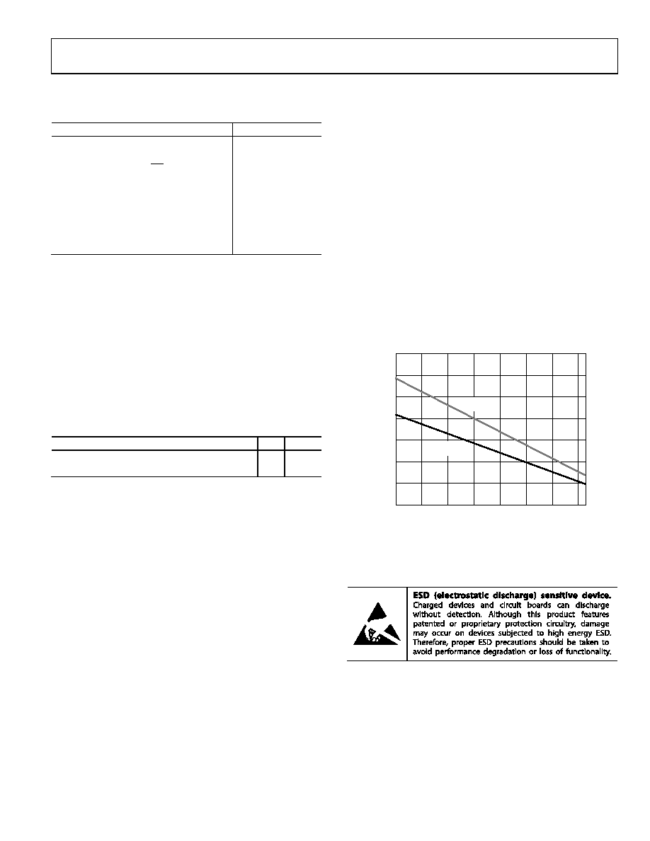
Figure 4 shows the maximum safe power dissipation in the
package vs. the ambient temperature for the single 16-lead
LFCSP (91°C/W) and the dual 24-lead LFCSP (65°C/W) on a
JEDEC standard 4-layer board with the exposed pad soldered to
a PCB pad that is connected to a solid plane.
3.5
0
0.5
1.0
1.5
2.0
2.5
3.0
–40
100
80
60
40
20
0
–20
MA
XI
MU
M
PO
W
ER
D
ISSI
PA
T
IO
N
(W
)
AMBIENT TEMPERATURE (°C)
ADA4932-1
ADA4932-2
07752-
204
Figure 4. Maximum Power Dissipation vs. Ambient Temperature for
a 4-Layer Board
ESD CAUTION
Rev. C | Page 7 of 28
相关PDF资料 |
PDF描述 |
|---|---|
| ADA4941-1YR-EBZ | BOARD EVAL FOR ADA4941-1YR |
| ADA4939-2YCP-EBZ | BOARD EVAL FOR ADA4939-2YCP |
| ADA4941-1YCP-EBZ | BOARD EVAL FOR ADA4941-1YCP |
| ADA4938-1YCP-EBZ | BOARD EVAL FOR ADA4938-1YCP |
| ADA4939-1YCP-EBZ | BOARD EVAL FOR ADA4939-1YCP |
相关代理商/技术参数 |
参数描述 |
|---|---|
| ADA4932-2YCPZ-R2 | 功能描述:IC AMP DIFF DUAL LP 80MA 24LFCSP RoHS:是 类别:集成电路 (IC) >> Linear - Amplifiers - Instrumentation 系列:- 标准包装:1,000 系列:- 放大器类型:电压反馈 电路数:4 输出类型:满摆幅 转换速率:33 V/µs 增益带宽积:20MHz -3db带宽:30MHz 电流 - 输入偏压:2nA 电压 - 输入偏移:3000µV 电流 - 电源:2.5mA 电流 - 输出 / 通道:30mA 电压 - 电源,单路/双路(±):4.5 V ~ 16.5 V,±2.25 V ~ 8.25 V 工作温度:-40°C ~ 85°C 安装类型:表面贴装 封装/外壳:14-SOIC(0.154",3.90mm 宽) 供应商设备封装:14-SOIC 包装:带卷 (TR) |
| ADA4932-2YCPZ-R2 | 制造商:Analog Devices 功能描述:IC DIFF AMP 560MHZ 2800V/ LFCSP-16 |
| ADA4932-2YCPZ-R21 | 制造商:AD 制造商全称:Analog Devices 功能描述:Low Power Differential ADC Driver |
| ADA4932-2YCPZ-R7 | 功能描述:IC AMP DIFF DUAL LP 80MA 24LFCSP RoHS:是 类别:集成电路 (IC) >> Linear - Amplifiers - Instrumentation 系列:- 标准包装:150 系列:- 放大器类型:音频 电路数:2 输出类型:- 转换速率:5 V/µs 增益带宽积:12MHz -3db带宽:- 电流 - 输入偏压:100nA 电压 - 输入偏移:500µV 电流 - 电源:6mA 电流 - 输出 / 通道:50mA 电压 - 电源,单路/双路(±):4 V ~ 32 V,±2 V ~ 16 V 工作温度:-40°C ~ 85°C 安装类型:表面贴装 封装/外壳:8-TSSOP(0.173",4.40mm 宽) 供应商设备封装:8-TSSOP 包装:管件 |
| ADA4932-2YCPZ-R71 | 制造商:AD 制造商全称:Analog Devices 功能描述:Low Power Differential ADC Driver |
发布紧急采购,3分钟左右您将得到回复。