- 您现在的位置:买卖IC网 > PDF目录16928 > ADA4939-1YCP-EBZ (Analog Devices Inc)BOARD EVAL FOR ADA4939-1YCP PDF资料下载
参数资料
| 型号: | ADA4939-1YCP-EBZ |
| 厂商: | Analog Devices Inc |
| 文件页数: | 11/24页 |
| 文件大小: | 0K |
| 描述: | BOARD EVAL FOR ADA4939-1YCP |
| 标准包装: | 1 |
| 每 IC 通道数: | 1 - 单 |
| 放大器类型: | 差分 |
| 板类型: | 裸(未填充) |
| 已供物品: | 板 |
| 已用 IC / 零件: | 16-LFCSP 封装 |
ADA4939-1/ADA4939-2
Rev. 0 | Page 19 of 24
Mismatched feedback networks also result in a degradation of
the ability of the circuit to reject input common-mode signals,
much the same as for a four-resistor difference amplifier made
from a conventional op amp.
As a practical summarization of the above issues, resistors of 1%
tolerance produce a worst-case input CMRR of approximately
40 dB, a worst-case differential-mode output offset of 25 mV
due to a 2.5 V VOCM input, negligible VOCM noise contribution,
and no significant degradation in output balance error.
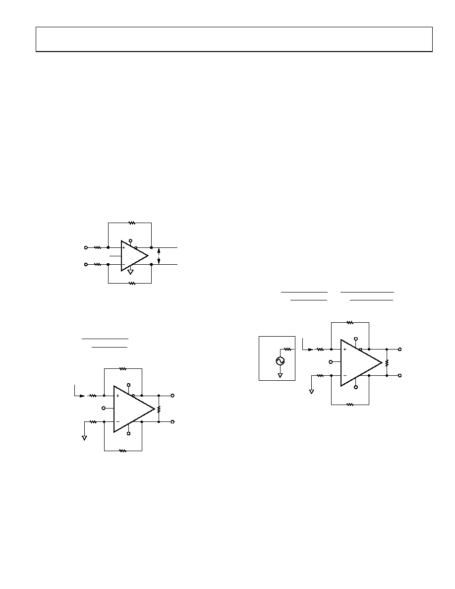
CALCULATING THE INPUT IMPEDANCE FOR AN
APPLICATION CIRCUIT
The effective input impedance of a circuit depends on whether
the amplifier is being driven by a single-ended or differential
signal source. For balanced differential input signals, as shown
(+DIN and DIN) is simply RIN, dm = 2 × RG.
+VS
ADA4939
+IN
–IN
RF
+DIN
–DIN
VOCM
RG
VOUT, dm
07
42
9-
0
51
Figure 44. ADA4939 Configured for Balanced (Differential) Inputs
For an unbalanced, single-ended input signal (see Figure 45),
the input impedance is
()
+
×
=
F
G
F
G
SE
IN
R
2
1
,
ADA4939
RL VOUT, dm
+VS
–VS
RG
RF
VOCM
RIN, SE
07
42
9-
0
52
Figure 45. ADA4939 with Unbalanced (Single-Ended) Input
The input impedance of the circuit is effectively higher than it
would be for a conventional op amp connected as an inverter
because a fraction of the differential output voltage appears at
the inputs as a common-mode signal, partially bootstrapping
the voltage across the input resistor RG. The common-mode
voltage at the amplifier input terminals can be easily determined by
noting that the voltage at the inverting input is equal to the
noninverting output voltage divided down by the voltage divider
formed by RF and RG in the lower loop. This voltage is present at
both input terminals due to negative voltage feedback and is in
phase with the input signal, thus reducing the effective voltage
across RG in the upper loop and partially bootstrapping RG.
Terminating a Single-Ended Input
This section deals with how to properly terminate a single-
ended input to the ADA4939 with a gain of 2, RF = 400 Ω, and
RG = 200 Ω. An example using an input source with a terminated
output voltage of 1 V p-p and source resistance of 50 Ω illustrates
the four simple steps that must be followed. Note that because
the terminated output voltage of the source is 1 V p-p, the open
circuit output voltage of the source is 2 V p-p. The source shown
in Figure 46 indicates this open-circuit voltage.
1.
The input impedance must be calculated using the formula
Ω
300
)
400
200
(
2
400
1
200
)
(
2
1
=
+
×
=
+
×
=
F
G
F
G
IN
R
RS
50
VS
2V p-p
RIN
300
ADA4939
RL VOUT, dm
+VS
–VS
RG
200
RG
200
RF
400
RF
400
VOCM
074
29
-05
3
Figure 46. Calculating Single-Ended Input Impedance RIN
相关PDF资料 |
PDF描述 |
|---|---|
| 4-1589788-9 | WDUALOBE CONNECTOR |
| VE-J4T-EY | CONVERTER MOD DC/DC 6.5V 50W |
| VE-J4R-EY | CONVERTER MOD DC/DC 7.5V 50W |
| VI-24R-EY | CONVERTER MOD DC/DC 7.5V 50W |
| GCC08DRYN-S734 | CONN EDGECARD 16POS DIP .100 SLD |
相关代理商/技术参数 |
参数描述 |
|---|---|
| ADA4939-1YCPZ-R2 | 制造商:Analog Devices 功能描述:SP Amp Differential ADC Driver Single 5.25V 16-Pin LFCSP EP T/R 制造商:Analog Devices 功能描述:SP AMP DIFFERENTIAL ADC DRVR SGL 5.25V 16LFCSP EP - Tape and Reel 制造商:Analog Devices 功能描述:SP Amp Differential ADC Driver Single 5.25V 16-Pin LFCSP EP Tape & Reel |
| ADA4939-1YCPZ-R7 | 功能描述:IC AMP DIFF ULDIST LN 16LFCSP RoHS:是 类别:集成电路 (IC) >> Linear - Amplifiers - Instrumentation 系列:- 标准包装:50 系列:- 放大器类型:J-FET 电路数:2 输出类型:- 转换速率:13 V/µs 增益带宽积:3MHz -3db带宽:- 电流 - 输入偏压:65pA 电压 - 输入偏移:3000µV 电流 - 电源:1.4mA 电流 - 输出 / 通道:- 电压 - 电源,单路/双路(±):7 V ~ 36 V,±3.5 V ~ 18 V 工作温度:-40°C ~ 85°C 安装类型:通孔 封装/外壳:8-DIP(0.300",7.62mm) 供应商设备封装:8-PDIP 包装:管件 |
| ADA4939-1YCPZ-RL | 功能描述:IC AMP DIFF ULDIST LN 16LFCSP RoHS:是 类别:集成电路 (IC) >> Linear - Amplifiers - Instrumentation 系列:- 标准包装:50 系列:- 放大器类型:J-FET 电路数:2 输出类型:- 转换速率:13 V/µs 增益带宽积:3MHz -3db带宽:- 电流 - 输入偏压:65pA 电压 - 输入偏移:3000µV 电流 - 电源:1.4mA 电流 - 输出 / 通道:- 电压 - 电源,单路/双路(±):7 V ~ 36 V,±3.5 V ~ 18 V 工作温度:-40°C ~ 85°C 安装类型:通孔 封装/外壳:8-DIP(0.300",7.62mm) 供应商设备封装:8-PDIP 包装:管件 |
| ADA4939-2 | 制造商:AD 制造商全称:Analog Devices 功能描述:Ultralow Distortion Differential ADC Driver |
| ADA4939-2YCP-EBZ | 功能描述:BOARD EVAL FOR ADA4939-2YCP RoHS:是 类别:编程器,开发系统 >> 评估板 - 运算放大器 系列:- 产品培训模块:Lead (SnPb) Finish for COTS Obsolescence Mitigation Program 标准包装:1 系列:- |
发布紧急采购,3分钟左右您将得到回复。