- 您现在的位置:买卖IC网 > PDF目录165344 > ADAU1382BCPZ (ANALOG DEVICES INC) SPECIALTY CONSUMER CIRCUIT, PQCC32 PDF资料下载
参数资料
| 型号: | ADAU1382BCPZ |
| 厂商: | ANALOG DEVICES INC |
| 元件分类: | 消费家电 |
| 英文描述: | SPECIALTY CONSUMER CIRCUIT, PQCC32 |
| 封装: | 5 X 5 MM, ROHS COMPLIANT, MO-220VHHD2, LFCSP-32 |
| 文件页数: | 29/84页 |
| 文件大小: | 1193K |
| 代理商: | ADAU1382BCPZ |
第1页第2页第3页第4页第5页第6页第7页第8页第9页第10页第11页第12页第13页第14页第15页第16页第17页第18页第19页第20页第21页第22页第23页第24页第25页第26页第27页第28页当前第29页第30页第31页第32页第33页第34页第35页第36页第37页第38页第39页第40页第41页第42页第43页第44页第45页第46页第47页第48页第49页第50页第51页第52页第53页第54页第55页第56页第57页第58页第59页第60页第61页第62页第63页第64页第65页第66页第67页第68页第69页第70页第71页第72页第73页第74页第75页第76页第77页第78页第79页第80页第81页第82页第83页第84页
ADAU1382
Rev. 0| Page 35 of 84
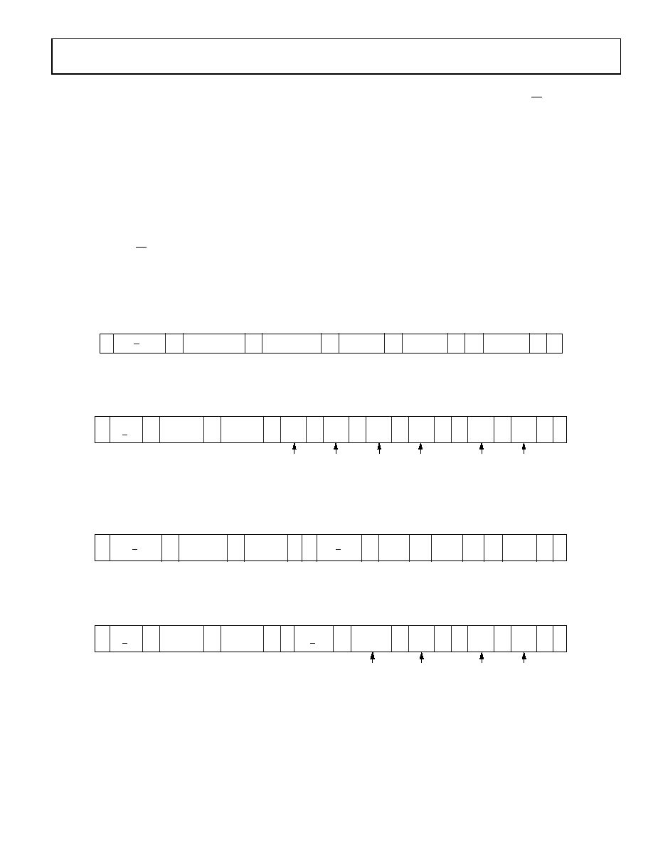
I2C Read and Write Operations
Figure 39 shows the timing of a single-word write operation.
Every ninth clock pulse, the ADAU1382 issues an acknowledge
by pulling SDA low.
Figure 40 shows the timing of a burst mode write sequence.
This figure shows an example where the target destination
registers are two bytes. The ADAU1382 knows to increment its
subaddress register every two bytes because the requested
subaddress corresponds to a register or memory area with a
2-byte word length.
The timing of a single-word read operation is shown in Figure 41.
Note that the first R/W bit is 0, indicating a write operation. This is
because the subaddress still needs to be written to set up the
internal address. After the ADAU1382 acknowledges the receipt
of the subaddress, the master must issue a repeated start command
followed by the chip address byte with the R/W bit set to 1 (read).
This causes the ADAU1382 SDA to reverse and begin driving
data back to the master. The master then responds every ninth
pulse with an acknowledge pulse to the ADAU1382.
Figure 42 shows the timing of a burst mode read sequence. This
figure shows an example where the target read registers are two
bytes. The ADAU1382 increments its subaddress every two bytes
because the requested subaddress corresponds to a register or
memory area with word lengths of two bytes. Other address
ranges may have a variety of word lengths ranging from one to
five bytes. The ADAU1382 always decodes the subaddress and
sets the auto-increment circuit so that the address increments
after the appropriate number of bytes.
S
AS
SUBADDRESS,
LOW BYTE
AS
...
AS
P
CHIP ADDRESS,
R/W = 0
DATA
BYTE 1
DATA
BYTE 2
DATA
BYTE N
SUBADDRESS,
HIGH BYTE
S = START BIT, P = STOP BIT, AS = ACKNOWLEDGE BY SLAVE.
SHOWS A ONE-WORD WRITE, WHERE EACH WORD HAS N BYTES.
08
427
-038
Figure 39. Single-Word I2C Write Sequence
S
AS
ASAS
AS
ASAS
AS
...
P
CHIP
ADDRESS,
R/W = 0
SUBADDRESS,
HIGH BYTE
SUBADDRESS,
LOW BYTE
DATA-WORD 1,
BYTE 1
DATA-WORD 1,
BYTE 2
DATA-WORD 2,
BYTE 1
DATA-WORD 2,
BYTE 2
DATA-WORD N,
BYTE 1
DATA-WORD N,
BYTE 2
S = START BIT, P = STOP BIT, AS = ACKNOWLEDGE BY SLAVE.
SHOWS AN N-WORD WRITE, WHERE EACH WORD HAS TWO BYTES. (OTHER WORD LENGTHS ARE POSSIBLE, RANGING FROM ONE TO FIVE BYTES.)
0
84
27
-0
39
Figure 40. Burst Mode I2C Write Sequence
S
AM
AS
AM
AS
S
AS
...
P
CHIP ADDRESS,
R/W = 0
CHIP ADDRESS,
R/W = 1
DATA
BYTE N
DATA
BYTE 2
DATA
BYTE 1
SUBADDRESS,
HIGH BYTE
SUBADDRESS,
LOW BYTE
S = START BIT, P = STOP BIT, AM = ACKNOWLEDGE BY MASTER, AS = ACKNOWLEDGE BY SLAVE.
SHOWS A ONE-WORD READ, WHERE EACH WORD HAS N BYTES.
08
42
7-
0
40
Figure 41. Single-Word I2C Read Sequence
S
SAS
AS
AM
...
P
CHIP
ADDRESS,
R/W = 0
SUBADDRESS,
HIGH BYTE
SUBADDRESS,
LOW BYTE
DATA-WORD 1,
BYTE 1
DATA-WORD 1,
BYTE 2
DATA-WORD N,
BYTE 1
DATA-WORD N,
BYTE 2
CHIP
ADDRESS,
R/W = 1
S = START BIT, P = STOP BIT, AM = ACKNOWLEDGE BY MASTER, AS = ACKNOWLEDGE BY SLAVE.
SHOWS AN N-WORD READ, WHERE EACH WORD HAS TWO BYTES. (OTHER WORD LENGTHS ARE POSSIBLE, RANGING FROM ONE TO FIVE BYTES.)
08
42
7-
0
41
Figure 42. Burst Mode I2C Read Sequence
相关PDF资料 |
PDF描述 |
|---|---|
| ADC-00403-103 | 1-CH 12-BIT SUCCESSIVE APPROXIMATION ADC, PARALLEL ACCESS, CDIP32 |
| ADC0831 | A/D Peripherals with Serial Control |
| ADC0831A | A/D Peripherals with Serial Control |
| ADC0831B | A/D Peripherals with Serial Control |
| ADC0832 | A/D Peripherals with Serial Control |
相关代理商/技术参数 |
参数描述 |
|---|---|
| ADAU1382BCPZ-R7 | 制造商:Analog Devices 功能描述:STEREO AUDIO CODEC FOR DIG STILL CAM - Tape and Reel 制造商:Analog Devices 功能描述:AUDIO CODEC |
| ADAU1401 | 制造商:AD 制造商全称:Analog Devices 功能描述:SigmaDSP 28-/56-Bit Audio Processor with Two ADCs and Four DACs |
| ADAU1401A | 制造商:AD 制造商全称:Analog Devices 功能描述:SigmaDSP 28-/56-Bit Audio Processor with Two ADCs and Four DACs |
| ADAU1401AWBSTZ | 功能描述:IC AUDIO PROC 28/56BIT 48LQFP RoHS:是 类别:集成电路 (IC) >> 线性 - 音频处理 系列:SigmaDSP® 其它有关文件:STA321 View All Specifications 标准包装:1 系列:Sound Terminal™ 类型:音频处理器 应用:数字音频 安装类型:表面贴装 封装/外壳:64-LQFP 裸露焊盘 供应商设备封装:64-LQFP EP(10x10) 包装:Digi-Reel® 其它名称:497-11050-6 |
| ADAU1401AWBSTZ-RL | 功能描述:IC AUDIO PROC 28/56BIT 48LQFP RoHS:是 类别:集成电路 (IC) >> 线性 - 音频处理 系列:SigmaDSP® 其它有关文件:STA321 View All Specifications 标准包装:1 系列:Sound Terminal™ 类型:音频处理器 应用:数字音频 安装类型:表面贴装 封装/外壳:64-LQFP 裸露焊盘 供应商设备封装:64-LQFP EP(10x10) 包装:Digi-Reel® 其它名称:497-11050-6 |
发布紧急采购,3分钟左右您将得到回复。