参数资料
| 型号: | ADAU1590ACPZ-RL7 |
| 厂商: | Analog Devices Inc |
| 文件页数: | 11/24页 |
| 文件大小: | 0K |
| 描述: | IC AMP AUDIO PWR 48LFCSP |
| 产品变化通告: | ADAU1513,1590 Discontinuation 09/Apr/2012 |
| 标准包装: | 750 |
| 类型: | D 类 |
| 输出类型: | 2 通道(立体声) |
| 在某负载时最大输出功率 x 通道数量: | 15.5W x 2 @ 4 欧姆 |
| 电源电压: | 9 V ~ 18 V |
| 特点: | 消除爆音,静音,待机,热保护 |
| 安装类型: | 表面贴装 |
| 供应商设备封装: | 48-LFCSP-VQ(7x7) |
| 封装/外壳: | 48-VFQFN 裸露焊盘,CSP |
| 包装: | 带卷 (TR) |
ADAU1590
Rev. 0 | Page 19 of 24
To shut down the power supplies, it is highly recommended to
mute the amplifier before shutting down any of the supplies.
After MUTE is shut down, shut down the supplies in the follow-
ing order: PVDD, DVDD, then AVDD. Where AVDD and
DVDD are generated from a single source, turn PVDD off
before DVDD and AVDD, and after issuing MUTE.
DC OFFSET AND POP NOISE
This section describes the cause of dc offset and pop noise
during turn-on/turn-off. The turn-on/turn-off pop in
amplifiers depend mainly on the dc offset, therefore, care must
be taken to reduce the dc offset at the output.
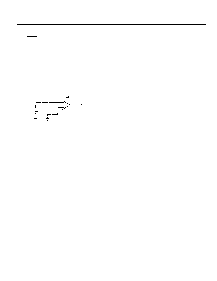
The first stage of ADAU1590 has an inverting PGA amplifier, as
shown in Figure 45.
0
66
73
-0
45
CHANGES WITH PGA SETTING
RFB
TO NEXT STAGE
AINx
VREF
CREF
RIN
RSOURCE
VMIS
CIN
Figure 45. Input Equivalent Circuit
where:
RIN = 20 kΩ, fixed internally.
RFB is the gain feedback resistor (value depends on the PGA
setting).
RSOURCE is the source resistance.
CIN is the input coupling capacitor (2.2 μF typical).
CREF is the filter capacitor for VREF.
VREF is the analog reference voltage (AVDD/2 typical).
VMIS is the dc offset due to mismatch in the op amp.
As shown in Figure 45, the dc offset at the output can be due to
VMIS (the dc offset from mismatch in the op amp) and due to
leakage current of the CIN capacitor.
Normally, the offset due to leakage current in the CIN is less and
can be ignored compared to VMIS. The VMIS is mainly responsi-
ble for the dc offset at the output. The ADAU1590 uses special
self-calibration or a dc offset trim circuit, which controls the dc
offset (due to VMIS) to within ±3 mV. The VMIS can vary for each
part as well as for voltage and temperature. The trim circuit
ensures that the offset is limited within specified limits and
provides virtually pop-free operation every time the part is
turned on. However, care must be taken while unmuting or
during the power-up sequence.
During the initial power-up, CIN and CREF are charging to
AVDD/2 and, during this time, there can be dc offset at the
output (see Figure 45). This depends on the PGA gain setting.
The dc offset is multiplied by the PGA gain setting. If the
amplifier is kept in mute during this charging and self-trimming
event for the recommended tWAIT time, the dc offset at the
output remains within ±3 mV. For more details on tWAIT, refer
to the Power-Up/Power-Down Sequence section.
The amount of pop at the turn-on depends on tWAIT, which in
turn depends on the values of CREF and CIN. The following
section describes how to select the value for the CREF and CIN.
SELECTING VALUE FOR CREF AND CIN
The CREF is the capacitor used for filtering the noise from
AVDD on VREF. VREF is used for the biasing of the internal
analog amplifier as well as the modulator. Therefore, care must
be taken to ensure that the recommended minimum value is
used. The minimum recommended value for CREF is 4.7 μF.
CIN is the input coupling capacitor and is used to decouple the
inputs from the external dc. The CIN value determines the low
corner frequency of the amplifier. It can be determined from
the following equation:
IN
LOW
C
R
f
×
π
×
=
2
1
where:
fLOW is the low corner frequency (3 dB).
RIN is the input resistance (20 kΩ).
CIN is the input coupling capacitor.
Note that RIN = 20 kΩ, provided that RSOURCE is <1 kΩ. If RSOURCE
is sizable with respect to RIN, it also must be taken into account
in calculation.
From the preceding equation, fLOW can be found for the desired
frequency response.
The recommended value for CIN is 2.2 μF, giving fLOW = 3.6 Hz,
and should keep 20 Hz roll-off within 0.5 dB.
However, if a higher than recommended CIN value is used for
better low frequency response, care must be taken to ensure
Sequence section for more details.
MONO MODE
The ADAU1590 mono mode can be enabled by pulling MO/ST
(Pin 11) to logic high. In this mode, the left channel input and
modulator is active and feeds PWM data to both the left and
right power stages. However, the respective power FETs need to
be connected externally for higher current capability. That is,
connect OUTL+ with OUTR+ and OUTL with OUTR. The
mono mode gives the capability to drive lower impedance loads
without invoking current limit. However, the output power is
limited by PVDD and temperature limits. See the typical applica-
tion schematic in Figure 47 for details.
POWER SUPPLY BYPASSING
Because Class-D amplifiers utilize high frequency switching,
care must be taken to bypassing the power supply.
For reliable operation, using 100 nF ceramic surface-mount
capacitors for the PVDD and PGND pins is recommended. The
minimum of two capacitors are needed: one between Pin 45/Pin 46
(PVDD) and Pin 47/Pin 48 (PGND), the other between Pin 39/
Pin 40 (PVDD) and Pin 37/Pin 38 (PGND). In addition, these
相关PDF资料 |
PDF描述 |
|---|---|
| ADAU1592ACPZ | IC AMP AUDIO PWR 24W 48LFCSP |
| ADAU1701JSTZ-RL | IC AUDIO PROC 2ADC/4DAC 48-LQFP |
| ADAU1702JSTZ-RL | IC AUDIO PROC 2ADC/4DAC 48-LQFP |
| ADAV4601BSTZ | IC AUDIO CODEC PROCESSOR 80-LQFP |
| ADAV4622BSTZ | IC AUD PRO ATV/SIF DECODE 80LQFP |
相关代理商/技术参数 |
参数描述 |
|---|---|
| ADAU1590ASVZ | 制造商:Analog Devices 功能描述: |
| ADAU1590ASVZ-RL | 制造商:AD 制造商全称:Analog Devices 功能描述:Class-D Audio Power Amplifier |
| ADAU1590ASVZRL7 | 制造商:AD 制造商全称:Analog Devices 功能描述:Class-D Audio Power Amplifier |
| ADAU1592 | 制造商:AD 制造商全称:Analog Devices 功能描述:Class-D Audio Power Amplifier |
| ADAU1592ACPZ | 功能描述:IC AMP AUDIO PWR 24W 48LFCSP RoHS:是 类别:集成电路 (IC) >> 线性 - 音頻放大器 系列:- 产品培训模块:Lead (SnPb) Finish for COTS Obsolescence Mitigation Program 标准包装:2,500 系列:DirectDrive® 类型:D 类 输出类型:1-通道(单声道),带立体声耳机 在某负载时最大输出功率 x 通道数量:930mW x 1 @ 8 欧姆; 40mW x 2 @ 16 欧姆 电源电压:2.7 V ~ 5.5 V 特点:消除爆音,差分输入,I²C,静音,关闭,音量控制 安装类型:表面贴装 供应商设备封装:25-WLP(2.09x2.09) 封装/外壳:25-WFBGA,WLCSP 包装:带卷 (TR) 其它名称:MAX97000EWA+T-ND |
发布紧急采购,3分钟左右您将得到回复。