- 您现在的位置:买卖IC网 > PDF目录10955 > ADAU1761BCPZ (Analog Devices Inc)IC SIGMADSP CODEC PLL 32LFCSP PDF资料下载
参数资料
| 型号: | ADAU1761BCPZ |
| 厂商: | Analog Devices Inc |
| 文件页数: | 17/92页 |
| 文件大小: | 0K |
| 描述: | IC SIGMADSP CODEC PLL 32LFCSP |
| 设计资源: | Stereo Digital Microphone Input Using ADAU1761 and ADMP421 (CN0078) |
| 标准包装: | 1 |
| 系列: | SigmaDSP® |
| 类型: | 音频编解码器 |
| 数据接口: | 串行 |
| 分辨率(位): | 24 b |
| ADC / DAC 数量: | 2 / 2 |
| 三角积分调变: | 是 |
| 电压 - 电源,模拟: | 1.8 V ~ 3.65 V |
| 电压 - 电源,数字: | 1.63V ~ 3.65V |
| 工作温度: | -40°C ~ 85°C |
| 安装类型: | 表面贴装 |
| 封装/外壳: | 32-VFQFN 裸露焊盘,CSP |
| 供应商设备封装: | 32-LFCSP-VQ |
| 包装: | 托盘 |
| 产品目录页面: | 776 (CN2011-ZH PDF) |
| 配用: | EVAL-ADAU1761Z-ND - BOARD EVAL FOR ADAU1761 |
第1页第2页第3页第4页第5页第6页第7页第8页第9页第10页第11页第12页第13页第14页第15页第16页当前第17页第18页第19页第20页第21页第22页第23页第24页第25页第26页第27页第28页第29页第30页第31页第32页第33页第34页第35页第36页第37页第38页第39页第40页第41页第42页第43页第44页第45页第46页第47页第48页第49页第50页第51页第52页第53页第54页第55页第56页第57页第58页第59页第60页第61页第62页第63页第64页第65页第66页第67页第68页第69页第70页第71页第72页第73页第74页第75页第76页第77页第78页第79页第80页第81页第82页第83页第84页第85页第86页第87页第88页第89页第90页第91页第92页
ADAU1761
Rev. C | Page 24 of 92
STARTUP, INITIALIZATION, AND POWER
This section describes the procedure for properly starting up
the ADAU1761. The following sequence provides a high level
approach to the proper initiation of the system.
1.
Apply power to the ADAU1761.
2.
Lock the PLL to the input clock (if using the PLL).
3.
Enable the core clock.
4.
Load the register settings.
See the Startup section for more information about the proper
start-up sequence.
POWER-UP SEQUENCE
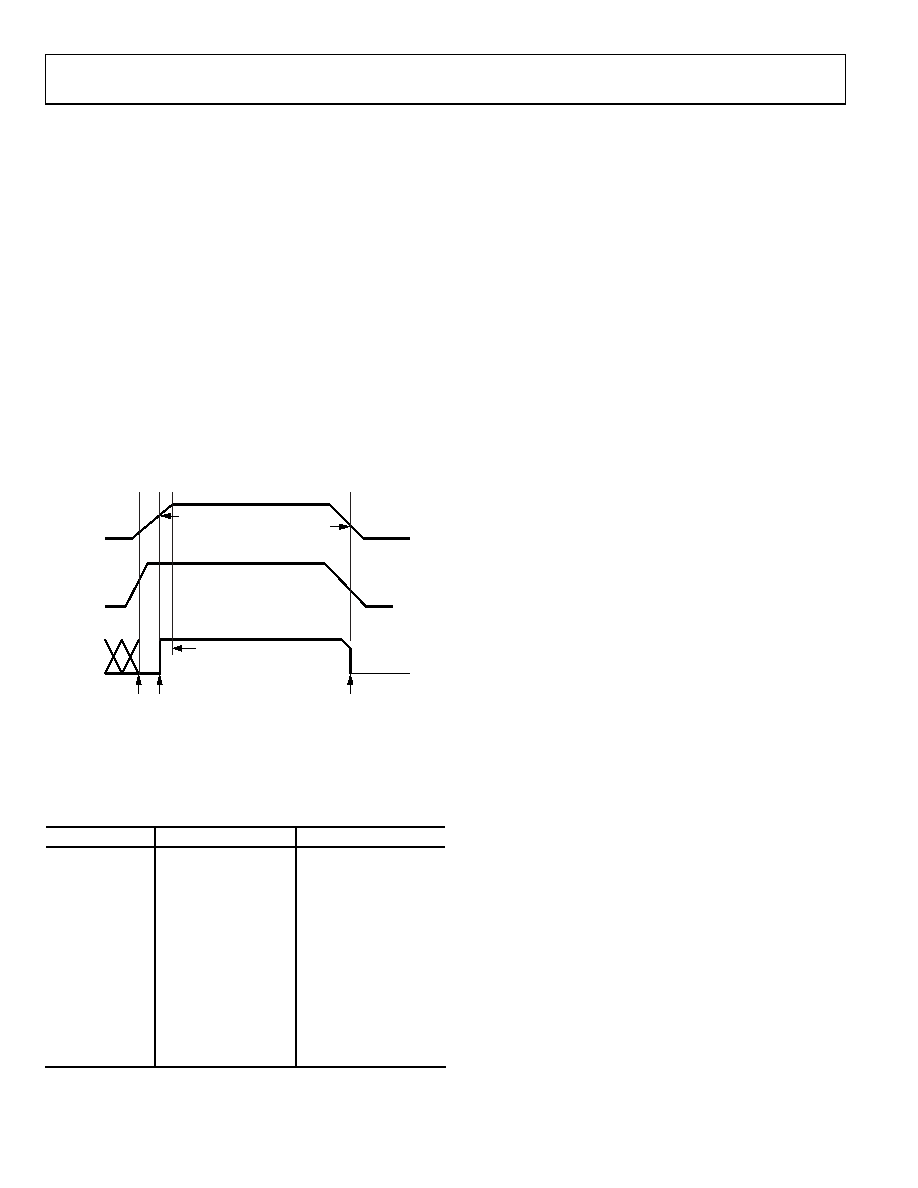
The ADAU1761 uses a power-on reset (POR) circuit to
reset the registers upon power-up. The POR monitors the
DVDDOUT pin and generates a reset signal whenever power
is applied to the chip. During the reset, the ADAU1761 is set
to the default values documented in the register map (see the
Control Registers section). Typically, with a 10 μF capacitor on
AVDD, the POR takes approximately 14 ms.
AVDD
POR
PART READY
POR
ACTIVE
POR ACTIVE
DVDDOUT
1.35V
0.95V
1.5V
POR
FINISHED
0
76
80
-0
61
Figure 29. Power-On Reset Sequence
The PLL lock time is dependent on the MCLK rate. Typical
lock times are provided in Table 11. The DSP can be enabled
immediately after the PLL is locked.
Table 11. PLL Lock Times
PLL Mode
MCLK Frequency
Lock Time (Typical)
Fractional
8 MHz
3.5 ms
Fractional
12 MHz
3.0 ms
Integer
12.288 MHz
2.96 ms
Fractional
13 MHz
2.4 ms
Fractional
14.4 MHz
2.4 ms
Fractional
19.2 MHz
2.98 ms
Fractional
19.68 MHz
2.98 ms
Fractional
19.8 MHz
2.98 ms
Fractional
24 MHz
2.95 ms
Integer
24.576 MHz
2.96 ms
Fractional
26 MHz
2.4 ms
Fractional
27 MHz
2.4 ms
POWER REDUCTION MODES
Sections of the ADAU1761 chip can be turned on and off as
needed to reduce power consumption. These include the ADCs,
the DACs, the PLL, and the DSP core.
In addition, the control registers can be used to configure some
functions for power saving, normal, or enhanced performance
operation. See the Control Registers section for more
information.
The digital filters of the ADCs and DACs can each be set to over-
sampling ratios of 64× or 128× (default). Setting the oversampling
ratios to 64× for these filters lowers power consumption with a
minimal impact on performance. See the Digital Filters section
for specifications; see the Typical Performance Characteristics
section for graphs of these filters.
DIGITAL POWER SUPPLY
The digital power supply for the ADAU1761 is generated from
an internal regulator. This regulator generates a 1.5 V supply
internally. The only external connection to this regulator is the
DVDDOUT bypassing point. A 100 nF capacitor and a 10 μF
capacitor should be connected between this pin and DGND.
INPUT/OUTPUT POWER SUPPLY
The power for the digital output pins is supplied from IOVDD,
and this pin also sets the highest input voltage that should be
seen on the digital input pins. IOVDD should be set between
1.8 V and 3.3 V; no digital input signal should be at a voltage
level higher than the one on IOVDD. The current draw of this
pin is variable because it depends on the loads of the digital
outputs. IOVDD should be decoupled to DGND with a 100 nF
capacitor and a 10 μF capacitor.
CLOCK GENERATION AND MANAGEMENT
The ADAU1761 uses a flexible clocking scheme that enables the
use of many different input clock rates. The PLL can be bypassed
or used, resulting in two different approaches to clock manage-
ment. For more information about clocking schemes, PLL
configuration, and sampling rates, see the Clocking and
Sampling Rates section.
Case 1: PLL Is Bypassed
If the PLL is bypassed, the core clock is derived directly from
the MCLK input. The rate of this clock must be set properly in
Register R0 (clock control register, Address 0x4000) using the
INFREQ[1:0] bits. When the PLL is bypassed, supported external
clock rates are 256 × fS, 512 × fS, 768 × fS, and 1024 × fS, where fS
is the base sampling rate. The core clock of the chip is off until
the core clock enable bit (COREN) is asserted. If a clock slower
than 1024 × fS is directly input to the ADAU1761 (bypassing the
PLL), the number of available SigmaDSP processing cycles is
reduced and the DSPSR bits in Register R57 (Address 0x40EB)
should be adjusted accordingly.
相关PDF资料 |
PDF描述 |
|---|---|
| MC9328MXSVP10R2 | IC MCU I.MXS 100MHZ 225-MAPBGA |
| MC9S12XEQ384CAG | MCU 16BIT 384K FLASH 144-LQFP |
| VE-B4W-IW-B1 | CONVERTER MOD DC/DC 5.5V 100W |
| MC705C8ACFNER | IC MCU 8BIT 44-PLCC |
| MC908GZ32MFAE | IC MCU 8BIT 32K FLASH 48-LQFP |
相关代理商/技术参数 |
参数描述 |
|---|---|
| ADAU1761BCPZ | 制造商:Analog Devices 功能描述:IC, AUDIO CODEC, 24BIT, 96KHZ, LFCSP-32 |
| ADAU1761BCPZ-R7 | 功能描述:IC SIGMADSP CODEC PLL 32LFCSP RoHS:是 类别:集成电路 (IC) >> 接口 - 编解码器 系列:SigmaDSP® 标准包装:2,500 系列:- 类型:立体声音频 数据接口:串行 分辨率(位):18 b ADC / DAC 数量:2 / 2 三角积分调变:是 S/N 比,标准 ADC / DAC (db):81.5 / 88 动态范围,标准 ADC / DAC (db):82 / 87.5 电压 - 电源,模拟:2.6 V ~ 3.3 V 电压 - 电源,数字:1.7 V ~ 3.3 V 工作温度:-40°C ~ 85°C 安装类型:表面贴装 封装/外壳:48-WFQFN 裸露焊盘 供应商设备封装:48-TQFN-EP(7x7) 包装:带卷 (TR) |
| ADAU1761BCPZ-RL | 功能描述:IC SIGMADSP CODEC PLL 32LFCSP RoHS:是 类别:集成电路 (IC) >> 接口 - 编解码器 系列:SigmaDSP® 标准包装:2,500 系列:- 类型:立体声音频 数据接口:串行 分辨率(位):18 b ADC / DAC 数量:2 / 2 三角积分调变:是 S/N 比,标准 ADC / DAC (db):81.5 / 88 动态范围,标准 ADC / DAC (db):82 / 87.5 电压 - 电源,模拟:2.6 V ~ 3.3 V 电压 - 电源,数字:1.7 V ~ 3.3 V 工作温度:-40°C ~ 85°C 安装类型:表面贴装 封装/外壳:48-WFQFN 裸露焊盘 供应商设备封装:48-TQFN-EP(7x7) 包装:带卷 (TR) |
| ADAU1772BCPZ | 功能描述:接口—CODEC Low Latency Noise and Power CODEC RoHS:否 制造商:Texas Instruments 类型: 分辨率: 转换速率:48 kSPs 接口类型:I2C ADC 数量:2 DAC 数量:4 工作电源电压:1.8 V, 2.1 V, 2.3 V to 5.5 V 最大工作温度:+ 85 C 安装风格:SMD/SMT 封装 / 箱体:DSBGA-81 封装:Reel |
| ADAU1772BCPZ-R7 | 功能描述:接口—CODEC Low Latency Noise and Power CODEC RoHS:否 制造商:Texas Instruments 类型: 分辨率: 转换速率:48 kSPs 接口类型:I2C ADC 数量:2 DAC 数量:4 工作电源电压:1.8 V, 2.1 V, 2.3 V to 5.5 V 最大工作温度:+ 85 C 安装风格:SMD/SMT 封装 / 箱体:DSBGA-81 封装:Reel |
发布紧急采购,3分钟左右您将得到回复。