- 您现在的位置:买卖IC网 > PDF目录10956 > ADAU1961WBCPZ (Analog Devices Inc)IC STEREO AUD CODEC LP 32LFCSP PDF资料下载
参数资料
| 型号: | ADAU1961WBCPZ |
| 厂商: | Analog Devices Inc |
| 文件页数: | 33/76页 |
| 文件大小: | 0K |
| 描述: | IC STEREO AUD CODEC LP 32LFCSP |
| 标准包装: | 1 |
| 类型: | 音频编解码器 |
| 数据接口: | I²C,串行,SPI? |
| 分辨率(位): | 24 b |
| ADC / DAC 数量: | 2 / 2 |
| 三角积分调变: | 无 |
| S/N 比,标准 ADC / DAC (db): | 98 / 98 |
| 动态范围,标准 ADC / DAC (db): | 96 / 98 |
| 电压 - 电源,模拟: | 2.97 V ~ 3.63 V |
| 电压 - 电源,数字: | 2.97 V ~ 3.63 V |
| 工作温度: | -40°C ~ 105°C |
| 安装类型: | 表面贴装 |
| 封装/外壳: | 32-VFQFN 裸露焊盘,CSP |
| 供应商设备封装: | 32-LFCSP-EP(5x5) |
| 包装: | 托盘 |
第1页第2页第3页第4页第5页第6页第7页第8页第9页第10页第11页第12页第13页第14页第15页第16页第17页第18页第19页第20页第21页第22页第23页第24页第25页第26页第27页第28页第29页第30页第31页第32页当前第33页第34页第35页第36页第37页第38页第39页第40页第41页第42页第43页第44页第45页第46页第47页第48页第49页第50页第51页第52页第53页第54页第55页第56页第57页第58页第59页第60页第61页第62页第63页第64页第65页第66页第67页第68页第69页第70页第71页第72页第73页第74页第75页第76页
Data Sheet
ADAU1961
Rev. A | Page 39 of 76
SPI PORT
By default, the ADAU1961 is in I2C mode, but it can be put into
SPI control mode by pulling CLATCH low three times. This is
done by performing three dummy writes to the SPI port (the
ADAU1961 does not acknowledge these three writes). Beginning
with the fourth SPI write, data can be written to or read from
the IC. The ADAU1961 can be taken out of SPI mode only by
a full reset initiated by power-cycling the IC.
The SPI port uses a 4-wire interface, consisting of the CLATCH,
CCLK, CDATA, and COUT signals, and it is always a slave port.
The CLATCH signal should go low at the beginning of a trans-
action and high at the end of a transaction. The CCLK signal
latches CDATA on a low-to-high transition. COUT data is shifted
out of the ADAU1961 on the falling edge of CCLK and should
be clocked into a receiving device, such as a microcontroller, on
the CCLK rising edge. The CDATA signal carries the serial input
data, and the COUT signal carries the serial output data. The
COUT signal remains three-state until a read operation is requested.
This allows other SPI-compatible peripherals to share the same
readback line. All SPI transactions have the same basic format
shown in Table 22. A timing diagram is shown in Figure 4. All
data should be written MSB first.
Chip Address R/W
The LSB of the first byte of an SPI transaction is a R/W bit. This bit
determines whether the communication is a read (Logic Level 1)
or a write (Logic Level 0). This format is shown in Table 21.
Table 21. ADAU1961 SPI Address and Read/Write Byte Format
Bit 0
Bit 1
Bit 2
Bit 3
Bit 4
Bit 5
Bit 6
Bit 7
0
R/W
Subaddress
The 16-bit subaddress word is decoded into a location in one of
the registers. This subaddress is the location of the appropriate
register. The MSBs of the subaddress are zero-padded to bring
the word to a full 2-byte length.
Data Bytes
The number of data bytes varies according to the register being
accessed. During a burst mode write, an initial subaddress is
written followed by a continuous sequence of data for consecu-
tive register locations.
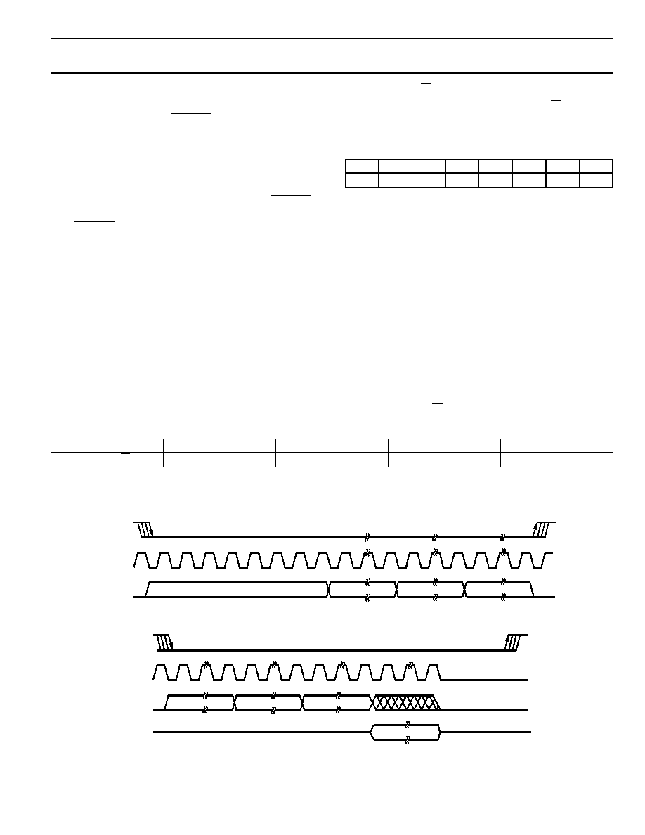
A sample timing diagram for a single-word SPI write operation
to a register is shown in Figure 54. A sample timing diagram of
a single-word SPI read operation is shown in Figure 55. The
COUT pin goes from being three-state to being driven at the
beginning of Byte 3. In this example, Byte 0 to Byte 2 contain
the addresses and R/W bit, and subsequent bytes carry the data.
Table 22. Generic Control Word Format
Byte 0
Byte 1
Byte 2
Byte 3
Byte 41
chip_adr[6:0], R/W
subaddr[15:8]
subaddr[7:0]
data
1 Continues to end of data.
CLATCH
CCLK
CDATA
BYTE 0
BYTE 1
BYTE 2
BYTE 3
0
891
5-
0
38
Figure 54. SPI Write to ADAU1961 Clocking (Single-Word Write Mode)
CLATCH
CCLK
CDATA
COUT
BYTE 0
BYTE 1
HIGH-Z
DATA
HIGH-Z
BYTE 2
08
91
5-
0
39
Figure 55. SPI Read from ADAU1961 Clocking (Single-Word Read Mode)
相关PDF资料 |
PDF描述 |
|---|---|
| MC908GZ60MFJE | IC MCU 8BIT 60K FLASH 32-LQFP |
| MC908GZ32VFJE | IC MCU 8BIT 32K FLASH 32-LQFP |
| AD74111YRUZ | IC CODEC AUDIO MONO LP 16TSSOP |
| VI-22R-IY-F3 | CONVERTER MOD DC/DC 7.5V 50W |
| CS4270-CZZ | IC CODEC 24BIT 105DB 24TSSOP |
相关代理商/技术参数 |
参数描述 |
|---|---|
| ADAU1961WBCPZ-R7 | 功能描述:IC STEREO AUD CODEC LP 32LFCSP RoHS:是 类别:集成电路 (IC) >> 接口 - 编解码器 系列:- 标准包装:2,500 系列:- 类型:立体声音频 数据接口:串行 分辨率(位):18 b ADC / DAC 数量:2 / 2 三角积分调变:是 S/N 比,标准 ADC / DAC (db):81.5 / 88 动态范围,标准 ADC / DAC (db):82 / 87.5 电压 - 电源,模拟:2.6 V ~ 3.3 V 电压 - 电源,数字:1.7 V ~ 3.3 V 工作温度:-40°C ~ 85°C 安装类型:表面贴装 封装/外壳:48-WFQFN 裸露焊盘 供应商设备封装:48-TQFN-EP(7x7) 包装:带卷 (TR) |
| ADAU1961WBCPZ-RL | 功能描述:IC STEREO AUD CODEC LP 32LFCSP RoHS:是 类别:集成电路 (IC) >> 接口 - 编解码器 系列:- 标准包装:2,500 系列:- 类型:立体声音频 数据接口:串行 分辨率(位):18 b ADC / DAC 数量:2 / 2 三角积分调变:是 S/N 比,标准 ADC / DAC (db):81.5 / 88 动态范围,标准 ADC / DAC (db):82 / 87.5 电压 - 电源,模拟:2.6 V ~ 3.3 V 电压 - 电源,数字:1.7 V ~ 3.3 V 工作温度:-40°C ~ 85°C 安装类型:表面贴装 封装/外壳:48-WFQFN 裸露焊盘 供应商设备封装:48-TQFN-EP(7x7) 包装:带卷 (TR) |
| ADAU1962AWBSTZ | 制造商:Analog Devices 功能描述:AUTOMOTIVE HIGH PERFORMANCE 12 DAC - Trays 制造商:Analog Devices 功能描述:IC DAC 80LQFP 制造商:Analog Devices 功能描述:DAC 24 BITS 48KHZ SPI LQFP 制造商:Analog Devices 功能描述:DAC, 24BIT, 192KSPS, LQFP-80, Resolution (Bits):24bit, Sampling Rate:192kSPS, Input Channel Type:Differential, Single Ended, Supply Voltage Range:3.14V to 3.46V, Digital IC Case Style:LQFP, No. of Pins:80, Data Interface:I2C, SPI |
| ADAU1962AWBSTZ-RL | 功能描述:24 Bit Digital to Analog Converter 12 80-LQFP (14x14) 制造商:analog devices inc. 系列:- 包装:带卷(TR) 零件状态:有效 位数:24 数模转换器数:12 建立时间:- 输出类型:Voltage - Unbuffered 差分输出:是 数据接口:I2C, SPI 参考类型:内部 电压 - 电源,模拟:3.14 V ~ 3.46 V 电压 - 电源,数字:2.25 V ~ 3.46 V INL/DNL(LSB):- 架构:三角积分 工作温度:-40°C ~ 125°C 封装/外壳:80-LQFP 供应商器件封装:80-LQFP(14x14) 标准包装:1,000 |
| ADAU1962WBSTZ | 功能描述:24 Bit Digital to Analog Converter 12 80-LQFP (14x14) 制造商:analog devices inc. 系列:- 包装:托盘 零件状态:有效 位数:24 数模转换器数:12 建立时间:- 输出类型:Voltage - Unbuffered 差分输出:是 数据接口:I2C, SPI 参考类型:内部 电压 - 电源,模拟:3.14 V ~ 3.46 V 电压 - 电源,数字:2.25 V ~ 3.46 V INL/DNL(LSB):- 架构:三角积分 工作温度:-40°C ~ 125°C 封装/外壳:80-LQFP 供应商器件封装:80-LQFP(14x14) 标准包装:90 |
发布紧急采购,3分钟左右您将得到回复。