- 您现在的位置:买卖IC网 > PDF目录357567 > ADC-207MC (MURATA POWER SOLUTIONS INC) PDF资料下载
参数资料
| 型号: | ADC-207MC |
| 厂商: | MURATA POWER SOLUTIONS INC |
| 元件分类: | ADC |
| 中文描述: | 1-CH 7-BIT FLASH METHOD ADC, PARALLEL ACCESS, CDIP18 |
| 封装: | ROHS COMPLIANT, CERAMIC, DIP-18 |
| 文件页数: | 3/6页 |
| 文件大小: | 210K |
| 代理商: | ADC-207MC |
OUTPUT CODING
(+REFERENCE = +5.12V –REFERENCE = ground, MIDPOINT = no connection)
NOTE: The reference should be held to ±0.1% accuracy or better. Do not use the +5V
power supply as a reference input without precision regulation and high frequency
decoupling.
Values shown here are for a +5.12V reference. Scale other references proportionally.
Calibration equipment should test for code changes at the midpoints between these
center values shown in Table 1. For example, at the half-scale major carry, set the
input to 2.54V and adjust the reference until the code flickers equally between 63 and
64. Note also that the weighting for the comparator resistor network leaves the first
and last thresholds within 1/2LSB of the end points to adjust the code transition to the
proper midpoint values.
two enable lines, CS1 and CS2. Table 2 shows the truth table for chip select
signals. CS1 has the function of enabling/disabling bits 1 through 7. CS2
has the function of enabling/disabling bits 1 through 7 and the overflow bit.
Also, a full-scale input produces all ones, including the overflow bit at the
output. The ADC-207 has an adjustable resistor ladder string. The top end,
idle point, and bottom end are brought out for use with applications circuits.
These pins are called +REFERENCE, MIDPOINT and –REFERENCE,
respectively. In typical operation +REFERENCE is tied to +5V, –REFERENCE
is tied to ground, and MIDPOINT is bypassed to ground. Such a configura-
tion results in a 0 to +5V input voltage range. The MIDPOINT pin can also
be tied to a +2.5V source to further improve integral linearity. This is usually
not necessary unless better than 7-bit linearity is needed.
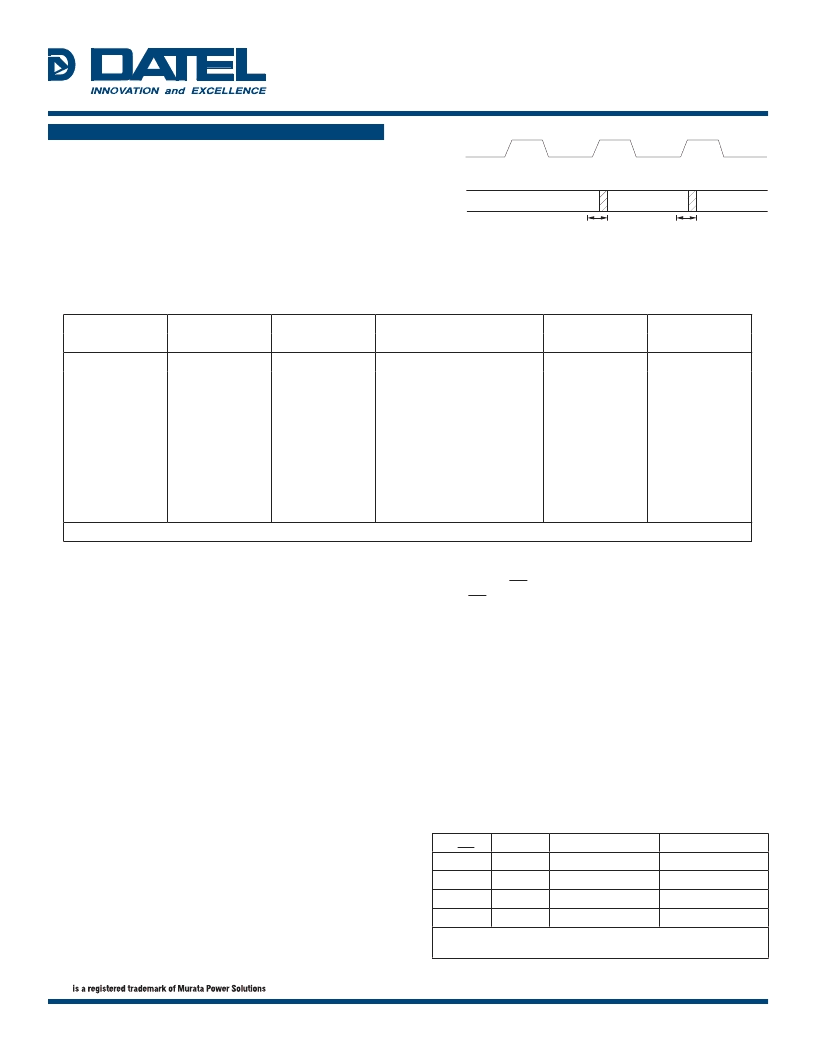
ADC-207 OPERATION
The ADC-207 uses a switched capacitor scheme in which there is an auto-
zero phase and a sampling phase. See
Figure 1 and Timing Diagram. The ADC-207 uses a single clock input.
When the clock is at a high state (logic 1), the ADC-207 is in the auto-zero
phase (1). When the clock is at a low state (logic 0), the ADC-207 is in
the sampling phase (2). During phase 1, the 128 comparator outputs are
shorted to their inputs through CMOS switches. This serves the purpose
of bringing the inputs and outputs to the transition levels of the respective
comparators. The inputs to the comparators are also connected to 128
sampling capacitors. The other end of the 128 capacitors are also shorted
to 128 taps of a resistor ladder, via CMOS switches. Therefore, during phase
1 the sampling capacitors are charged to the differential voltage between a
resistor tap and its respective comparator transition voltage.
This eliminates offset differences between comparators and yields better
temperature performance. During phase 2 (2) the input voltage is applied to
the 128 capacitors, via CMOS switches. This forces the comparators to trip
either high or low. Since the comparators during phase 1 were sitting at their
transition point, they can trip very quickly to the correct state. Also during
phase 2, the outputs of the comparators are loaded into internal latches
which in turn feed a128-to-7 encoder. When going back into phase 1, the
output of the encoder is loaded into an output latch. This latch then feeds the
3-state output buffer.
This means that the ADC-207 is of pipeline design. To do a single con-
version, the ADC-207 requires a positive pulse followed by a negative pulse
followed by a positive pulse. Continuous conversion requires one cycle/
sample (one positive pulse and one negative pulse). The 3-state buffer has
CLOCK
OUTPUT
DATA
AUTO
ZERO
N DATA
N+1 DATA
SAMPLE
N
SAMPLE
N + 1
SAMPLE
N + 2
AUTO
ZERO
AUTO
ZERO
17ns max.
17ns max.
1
2
1
1
2
2
TIMING DIAGRAM
Analog Input
(Center Value)
Code
Overflow
1
2
3
4
5
6
7
Decimal
Hexadecimal
(Incl. 0V)
MSB
LSB
0.00V
Zero
0
0
0
0
0
0
0
0
0
00
+0.04V
+1LSB
0
0
0
0
0
0
0
1
1
01
+1.28V
+1/4FS
0
0
1
0
0
0
0
0
32
20
+2.52V
+1/2FS – 1LSB
0
0
1
1
1
1
1
1
63
3F
+2.56V
+1/2FS
0
1
0
0
0
0
0
0
64
40
+2.60V
+1/2FS + 1LSB
0
1
0
0
0
0
0
1
65
41
+3.84V
+3/4FS
0
1
1
0
0
0
0
0
96
60
+5.08V
+FS
0
1
1
1
1
1
1
1
127
7F
+5.12V
Overflow
1
1
1
1
1
1
1
1
255*
FF
*Note that the overflow code does not clear the data bits.
Table 1. ADC-207 Output Coding
Table 2. Chip Select Truth Table
CS1
CS2
Bits 1-7
Overflow Bit
0
0
3-State Mode
3-State Mode
1
0
3-State Mode
3-State Mode
0
1
Data Outputed
Data Outputed
1
1
3-State Mode
Data Outputed
NOTE: Reduce the sample time (sample pulse) o 12ns to improve performance
above 20MHz. Such a configuration will closely esemble an ideal sampler.
ADC-207
7-Bit, 20MHz, CMOS Flash A/D Converters
DATEL
11 Cabot Boulevard, Mansfield, MA 02048-1151 USA Tel: (508) 339-3000 www.datel.com e-mail: help@datel.com
30 Mar 2011 MDA_ADC-207.B02
Page 3 of 6
相关PDF资料 |
PDF描述 |
|---|---|
| ADE05 | SLIDE DIP SWITCH-5SWITCHES, SPST, LATCHED,THROUGH HOLE-STRAIGHT |
| ADE06SA | SLIDE DIP SWITCH-6SWITCHES, SPST, LATCHED,SURFACE MOUNT-STRAIGHT |
| ADF0204 | SLIDE DIP SWITCH-2SWITCHES, SPST, LATCHED,0.1A, 24VDC, THROUGH HOLE-STRAIGHT |
| ADF03 | SLIDE DIP SWITCH-3SWITCHES, SPST, LATCHED,THROUGH HOLE-STRAIGHT |
| ADF07T | SLIDE DIP SWITCH-7SWITCHES, SPST, LATCHED,THROUGH HOLE-STRAIGHT |
相关代理商/技术参数 |
参数描述 |
|---|---|
| ADC-207MM | 制造商:Murata Power Solutions 功能描述:ADC Single Flash 20Msps 7-bit Parallel 18-Pin CDIP |
| ADC-207MM-QL | 制造商:Murata Power Solutions 功能描述:ADC Single Flash 20Msps 7-bit Parallel 18-Pin CDIP |
| ADC208 | 制造商:MPSIND 制造商全称:MPS Industries, Inc. 功能描述:1W, High Isolation SIP, Single & Dual Output DC/DC Converters |
| ADC-208A | 制造商:MURATA-PS 制造商全称:Murata Power Solutions Inc. 功能描述:8-Bit, 20MSPS CMOS Flash A/D (ADC-208 Compatible) |
| ADC-208ALC | 制造商:Murata Power Solutions 功能描述:ADC Single Flash 20Msps 8-bit Parallel 24-Pin CLCC |
发布紧急采购,3分钟左右您将得到回复。