- 您现在的位置:买卖IC网 > PDF目录378277 > ADC0801 (National Semiconductor Corporation) 8-Bit uP Compatible A/D Converters PDF资料下载
参数资料
| 型号: | ADC0801 |
| 厂商: | National Semiconductor Corporation |
| 元件分类: | 串行ADC |
| 英文描述: | 8-Bit uP Compatible A/D Converters |
| 中文描述: | 8位的兼容的A / D转换器 |
| 文件页数: | 17/41页 |
| 文件大小: | 1118K |
| 代理商: | ADC0801 |
第1页第2页第3页第4页第5页第6页第7页第8页第9页第10页第11页第12页第13页第14页第15页第16页当前第17页第18页第19页第20页第21页第22页第23页第24页第25页第26页第27页第28页第29页第30页第31页第32页第33页第34页第35页第36页第37页第38页第39页第40页第41页
Functional Description
(Continued)
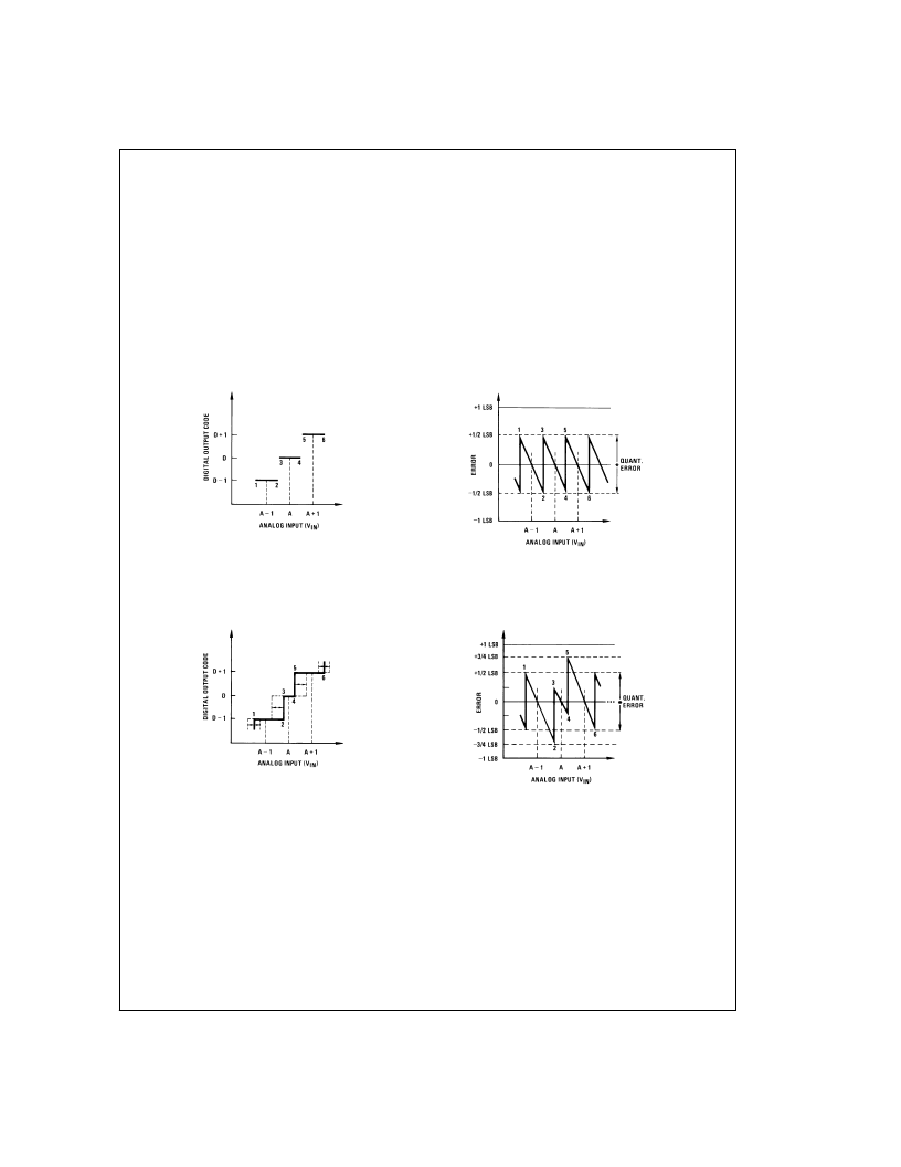
Figure 2 shows a worst case error plot for the ADC0801. All
center-valued inputs are guaranteed to produce the correct
output codes and the adjacent risers are guaranteed to be
no closer to the center-value points than
±
1
4
LSB. In other
words, if we apply an analog input equal to the center-value
±
1
4
LSB, we guarantee that the A/D will produce the correct
digital code. The maximum range of the position of the code
transition is indicated by the horizontal arrow and it is guar-
anteed to be no more than
1
2
LSB.
The error curve of Figure 3 shows a worst case error plot for
the ADC0802. Here we guarantee that if we apply an analog
input equal to the LSB analog voltage center-value the A/D
will produce the correct digital code.
Next to each transfer function is shown the corresponding
error plot. Many people may be more familiar with error plots
than transfer functions. The analog input voltage to the A/D
is provided by either a linear ramp or by the discrete output
steps of a high resolution DAC. Notice that the error is con-
tinuously displayed and includes the quantization uncertainty
of the A/D. For example the error at point 1 of Figure 1is +
1
2
LSB because the digital code appeared
1
2
LSB in advance
of the center-value of the tread. The error plots always have
a constant negative slope and the abrupt upside steps are
always 1 LSB in magnitude.
Transfer Function
DS005671-81
Error Plot
DS005671-82
FIGURE 1. Clarifying the Error Specs of an A/D Converter
Accuracy=
±
0 LSB: A Perfect A/D
Transfer Function
DS005671-83
Error Plot
DS005671-84
FIGURE 2. Clarifying the Error Specs of an A/D Converter
Accuracy=
±
1
4
LSB
A
www.national.com
17
相关PDF资料 |
PDF描述 |
|---|---|
| ADC0802 | 8-Bit uP Compatible A/D Converters |
| ADC0802LCN | 8-Bit uP Compatible A/D Converters |
| ADC0805 | 8-Bit uP Compatible A/D Converters |
| ADC0802LCWM | 8-Bit uP Compatible A/D Converters |
| ADC0801LCN | 8-Bit uP Compatible A/D Converters |
相关代理商/技术参数 |
参数描述 |
|---|---|
| ADC0801_1 | 制造商:NSC 制造商全称:National Semiconductor 功能描述:8-Bit μP Compatible A/D Converters |
| ADC0801IN | 制造商:未知厂家 制造商全称:未知厂家 功能描述:Analog-to-Digital Converter, 8-Bit |
| ADC0801LCD/A+ | 制造商:未知厂家 制造商全称:未知厂家 功能描述:Analog-to-Digital Converter, 8-Bit |
| ADC0801LCJ | 制造商:NSC 制造商全称:National Semiconductor 功能描述:8-Bit uP Compatible A/D Converters |
| ADC0801LCJ/A+ | 制造商:未知厂家 制造商全称:未知厂家 功能描述:Analog-to-Digital Converter, 8-Bit |
发布紧急采购,3分钟左右您将得到回复。