- 您现在的位置:买卖IC网 > PDF目录378277 > ADC0801LCN (NATIONAL SEMICONDUCTOR CORP) 8-Bit uP Compatible A/D Converters PDF资料下载
参数资料
| 型号: | ADC0801LCN |
| 厂商: | NATIONAL SEMICONDUCTOR CORP |
| 元件分类: | ADC |
| 英文描述: | 8-Bit uP Compatible A/D Converters |
| 中文描述: | 1-CH 8-BIT SUCCESSIVE APPROXIMATION ADC, PARALLEL ACCESS, PDIP20 |
| 封装: | PLASTIC, DIP-20 |
| 文件页数: | 33/41页 |
| 文件大小: | 1118K |
| 代理商: | ADC0801LCN |
第1页第2页第3页第4页第5页第6页第7页第8页第9页第10页第11页第12页第13页第14页第15页第16页第17页第18页第19页第20页第21页第22页第23页第24页第25页第26页第27页第28页第29页第30页第31页第32页当前第33页第34页第35页第36页第37页第38页第39页第40页第41页
Functional Description
(Continued)
Note 25:
In order for the microprocessor to service subroutines and interrupts, the stack pointer must be dimensioned in the user’s program.
For amplification of DC input signals, a major system error is
the input offset voltage of the amplifiers used for the preamp.
Figure 18 is a gain of 100 differential preamp whose offset
voltage errors will be cancelled by a zeroing subroutine
which is performed by the INS8080A microprocessor sys-
tem. The total allowable input offset voltage error for this
preamp is only 50 μV for
1
4
LSB error. This would obviously
require very precise amplifiers. The expression for the differ-
ential output voltage of the preamp is:
where I
is the current through resistor R
X
. All of the offset
error terms can be cancelled by making
±
I
R
= V
+
V
V
OS2
. This is the principle of this auto-zeroing
scheme.
The INS8080A uses the 3 I/O ports of an INS8255 Program-
able Peripheral Interface (PPI) to control the auto zeroing
and input data from the ADC0801 as shown in Figure 19
The PPI is programmed for basic I/O operation (mode 0) with
Port A being an input port and Ports B and C being output
ports. Two bits of Port C are used to alternately open or close
the 2 switches at the input of the preamp. Switch SW1 is
closed to force the preamp’s differential input to be zero dur-
ing the zeroing subroutine and then opened and SW2 is then
closed for conversion of the actual differential input signal.
Using 2 switches in this manner eliminates concern for the
ON resistance of the switches as they must conduct only the
input bias current of the input amplifiers.
Output Port B is used as a successive approximation regis-
ter by the 8080 and the binary scaled resistors in series with
each output bit create a D/A converter. During the zeroing
subroutine, the voltage at V
increases or decreases as re-
quired to make the differential output voltage equal to zero.
This is accomplished by ensuring that the voltage at the out-
put of A1 is approximately 2.5V so that a logic “1” (5V) on
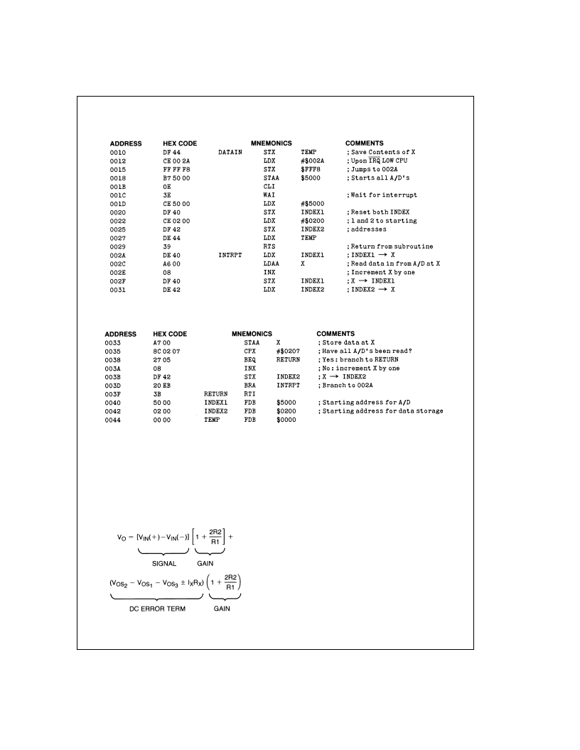
SAMPLE PROGRAM FOR
Figure 17
INTERFACING MULTIPLE A/D’s IN AN MC6800 SYSTEM
DS005671-A3
SAMPLE PROGRAM FOR
Figure 17
INTERFACING MULTIPLE A/D’s IN AN MC6800 SYSTEM
DS005671-A4
A
www.national.com
33
相关PDF资料 |
PDF描述 |
|---|---|
| ADC0802 | 8-Bit, Microprocessor- Compatible, A/D Converters |
| ADC0802LCD | 8-Bit, Microprocessor- Compatible, A/D Converters |
| ADC0802LCN | 8-Bit, Microprocessor- Compatible, A/D Converters |
| ADC0802LD | 8-Bit, Microprocessor- Compatible, A/D Converters |
| ADC0804 | 8-Bit, Microprocessor-Compatible A/D Converters |
相关代理商/技术参数 |
参数描述 |
|---|---|
| ADC0801LCN/A+ | 制造商:未知厂家 制造商全称:未知厂家 功能描述:Analog-to-Digital Converter, 8-Bit |
| ADC0801LCN/NOPB | 功能描述:模数转换器 - ADC RoHS:否 制造商:Texas Instruments 通道数量:2 结构:Sigma-Delta 转换速率:125 SPs to 8 KSPs 分辨率:24 bit 输入类型:Differential 信噪比:107 dB 接口类型:SPI 工作电源电压:1.7 V to 3.6 V, 2.7 V to 5.25 V 最大工作温度:+ 85 C 安装风格:SMD/SMT 封装 / 箱体:VQFN-32 |
| ADC0801LCNNOPB | 制造商:NATIONAL SEMICONDUCTOR 功能描述:_ |
| ADC0801LJ | 制造商:NSC 制造商全称:National Semiconductor 功能描述:8-Bit uP Compatible A/D Converters |
| ADC0801S040 | 制造商:PHILIPS 制造商全称:NXP Semiconductors 功能描述:Single 8 bits ADC, up to 40 MHz |
发布紧急采购,3分钟左右您将得到回复。