- 您现在的位置:买卖IC网 > PDF目录378277 > ADC0802 (National Semiconductor Corporation) 8-Bit uP Compatible A/D Converters PDF资料下载
参数资料
| 型号: | ADC0802 |
| 厂商: | National Semiconductor Corporation |
| 元件分类: | 串行ADC |
| 英文描述: | 8-Bit uP Compatible A/D Converters |
| 中文描述: | 8位的兼容的A / D转换器 |
| 文件页数: | 35/41页 |
| 文件大小: | 1118K |
| 代理商: | ADC0802 |
第1页第2页第3页第4页第5页第6页第7页第8页第9页第10页第11页第12页第13页第14页第15页第16页第17页第18页第19页第20页第21页第22页第23页第24页第25页第26页第27页第28页第29页第30页第31页第32页第33页第34页当前第35页第36页第37页第38页第39页第40页第41页
Functional Description
(Continued)
A flow chart for the zeroing subroutine is shown in Figure 20
It must be noted that the ADC0801 series will output an all
zero code when it converts a negative input [V
()
≥
V
(+)].
Also, a logic inversion exists as all of the I/O ports are buff-
ered with inverting gates.
Basically, if the data read is zero, the differential output volt-
age is negative, so a bit in Port B is cleared to pull V
more
negative which will make the output more positive for the
next conversion. If the data read is not zero, the output volt-
age is positive so a bit in Port B is set to make V
more posi-
tive and the output more negative. This continues for 8 ap-
proximations
and
the
differential
converges to within 5 mV of zero.
The actual program is given in Figure 21All addresses used
are compatible with the BLC 80/10 microcomputer system.
In particular:
Port A and the ADC0801 are at port address E4
Port B is at port address E5
Port C is at port address E6
PPI control word port is at port address E7
Program Counter automatically goes toADDR:3C3D upon
acknowledgement of an interrupt from the ADC0801
output
eventually
5.3 Multiple A/D Converters in a Z-80 Interrupt
Driven Mode
In data acquisition systems where more than one A/D con-
verter (or other peripheral device) will be interrupting pro-
gram execution of a microprocessor, there is obviously a
need for the CPU to determine which device requires servic-
ing. Figure 22 and the accompanying software is a method
of determining which of 7 ADC0801 converters has com-
pleted a conversion (INTR asserted) and is requesting an in-
terrupt. This circuit allows starting the A/D converters in any
sequence, but will input and store valid data from the con-
verters with a priority sequence of A/D 1 being read first, A/D
2 second, etc., through A/D 7 which would have the lowest
priority for data being read. Only the converters whose INT is
asserted will be read.
The key to decoding circuitry is the DM74LS373, 8-bit D type
flip-flop. When the Z-80 acknowledges the interrupt, the pro-
gram is vectored to a data input Z-80 subroutine. This sub-
routine will read a peripheral status word from the
DM74LS373 which contains the logic state of the INTR out-
puts of all the converters. Each converter which initiates an
interrupt will place a logic “0” in a unique bit position in the
status word and the subroutine will determine the identity of
the converter and execute a data read. An identifier word
(which indicates which A/D the data came from) is stored in
the next sequential memory location above the location of
the data so the program can keep track of the identity of the
data entered.
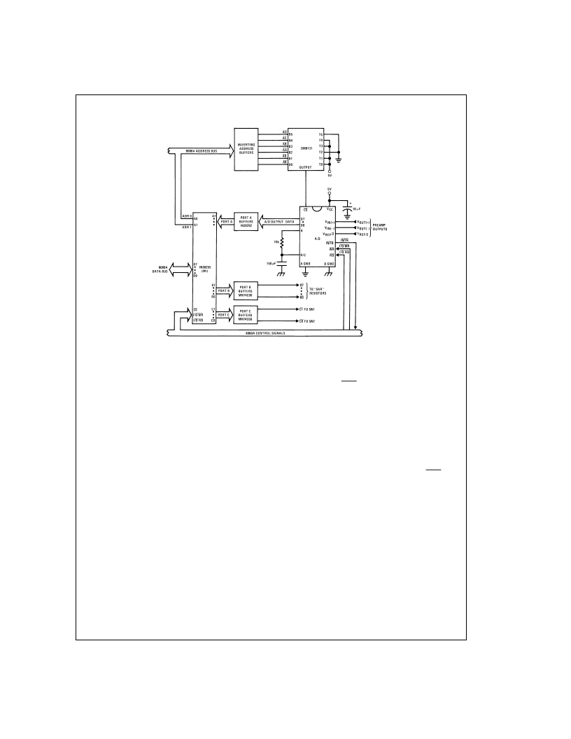
DS005671-92
FIGURE 19. Microprocessor Interface Circuitry for Differential Preamp
A
www.national.com
35
相关PDF资料 |
PDF描述 |
|---|---|
| ADC0802LCN | 8-Bit uP Compatible A/D Converters |
| ADC0805 | 8-Bit uP Compatible A/D Converters |
| ADC0802LCWM | 8-Bit uP Compatible A/D Converters |
| ADC0801LCN | 8-Bit uP Compatible A/D Converters |
| ADC0802 | 8-Bit, Microprocessor- Compatible, A/D Converters |
相关代理商/技术参数 |
参数描述 |
|---|---|
| ADC0802LCD | 制造商:INTERSIL 制造商全称:Intersil Corporation 功能描述:8-Bit, Microprocessor- Compatible, A/D Converters |
| ADC0802LCD/A+ | 制造商:未知厂家 制造商全称:未知厂家 功能描述:Analog-to-Digital Converter, 8-Bit |
| ADC0802LCJ | 制造商:NSC 制造商全称:National Semiconductor 功能描述:8-Bit uP Compatible A/D Converters |
| ADC0802LCJ/A+ | 制造商:未知厂家 制造商全称:未知厂家 功能描述:Analog-to-Digital Converter, 8-Bit |
| ADC0802LCN | 功能描述:模数转换器 - ADC RoHS:否 制造商:Texas Instruments 通道数量:2 结构:Sigma-Delta 转换速率:125 SPs to 8 KSPs 分辨率:24 bit 输入类型:Differential 信噪比:107 dB 接口类型:SPI 工作电源电压:1.7 V to 3.6 V, 2.7 V to 5.25 V 最大工作温度:+ 85 C 安装风格:SMD/SMT 封装 / 箱体:VQFN-32 |
发布紧急采购,3分钟左右您将得到回复。