- 您现在的位置:买卖IC网 > PDF目录378277 > ADC0802LD (HARRIS SEMICONDUCTOR) 8-Bit, Microprocessor- Compatible, A/D Converters PDF资料下载
参数资料
| 型号: | ADC0802LD |
| 厂商: | HARRIS SEMICONDUCTOR |
| 元件分类: | ADC |
| 英文描述: | 8-Bit, Microprocessor- Compatible, A/D Converters |
| 中文描述: | 1-CH 8-BIT SUCCESSIVE APPROXIMATION ADC, PARALLEL ACCESS, CDIP20 |
| 文件页数: | 20/41页 |
| 文件大小: | 1118K |
| 代理商: | ADC0802LD |
第1页第2页第3页第4页第5页第6页第7页第8页第9页第10页第11页第12页第13页第14页第15页第16页第17页第18页第19页当前第20页第21页第22页第23页第24页第25页第26页第27页第28页第29页第30页第31页第32页第33页第34页第35页第36页第37页第38页第39页第40页第41页
Functional Description
(Continued)
2.2 Analog Differential Voltage Inputs and
Common-Mode Rejection
ThisA/D has additional applications flexibility due to the ana-
log differential voltage input. The V
() input (pin 7) can be
used to automatically subtract a fixed voltage value from the
input reading (tare correction). This is also useful in 4 mA–20
mA current loop conversion. In addition, common-mode
noise can be reduced by use of the differential input.
The time interval between sampling V
(+) and V
() is 4-
1
2
clock periods. The maximum error voltage due to this slight
time difference between the input voltage samples is given
by:
where:
V
e
is the error voltage due to sampling delay
V
P
is the peak value of the common-mode voltage
f
cm
is the common-mode frequency
As an example, to keep this error to
1
4
LSB (
~
5 mV) when
operating with a 60 Hz common-mode frequency, f
, and
using a 640 kHz A/D clock, f
CLK
, would allow a peak value of
the common-mode voltage, V
P
, which is given by:
or
which gives
V
P
1.9V.
The allowed range of analog input voltages usually places
more severe restrictions on input common-mode noise lev-
els.
An analog input voltage with a reduced span and a relatively
large zero offset can be handled easily by making use of the
differential input (see section 2.4 Reference Voltage).
2.3 Analog Inputs
2.3 1 Input Current
Normal Mode
Due to the internal switching action, displacement currents
will flow at the analog inputs. This is due to on-chip stray ca-
pacitance to ground as shown in Figure 5
The voltage on this capacitance is switched and will result in
currents entering the V
(+) input pin and leaving the V
()
input which will depend on the analog differential input volt-
age levels. These current transients occur at the leading
edge of the internal clocks. They rapidly decay and do not
cause errorsas the on-chip comparator is strobed at the end
of the clock period.
Fault Mode
If the voltage source applied to the V
IN
(+) or V
() pin ex-
ceeds the allowed operating range of V
+50 mV, large in-
put currents can flow through a parasitic diode to the V
pin. If these currents can exceed the 1 mA max allowed
spec, an external diode (1N914) should be added to bypass
this current to the V
pin (with the current bypassed with
this diode, the voltage at the V
(+) pin can exceed the V
CC
voltage by the forward voltage of this diode).
2.3.2 Input Bypass Capacitors
Bypass capacitors at the inputs will average these charges
and cause a DC current to flow through the output resis-
tances of the analog signal sources. This charge pumping
action is worse for continuous conversions with the V
(+) in-
put voltage at full-scale. For continuous conversions with a
640 kHz clock frequency with the V
(+) input at 5V, this DC
current is at a maximum of approximately 5 μA. Therefore,
bypass capacitors should not be used at the analog inputs or
the V
/2 pin for high resistance sources (
>
1 k
). If input
bypass capacitors are necessary for noise filtering and high
source resistance is desirable to minimize capacitor size, the
detrimental effects of the voltage drop across this input resis-
tance, which is due to the average value of the input current,
can be eliminated with a full-scale adjustment while the
given source resistor and input bypass capacitor are both in
place. This is possible because the average value of the in-
put current is a precise linear function of the differential input
voltage.
2.3.3 Input Source Resistance
Large values of source resistance where an input bypass ca-
pacitor is not used, will not cause errorsas the input currents
settle out prior to the comparison time. If a low pass filter is
required in the system, use a low valued series resistor
(
≤
1 k
) for a passive RC section or add an op amp RC ac-
tive low pass filter. For low source resistance applications,
(
≤
1 k
), a 0.1 μF bypass capacitor at the inputs will prevent
noise pickup due to series lead inductance of a long wire. A
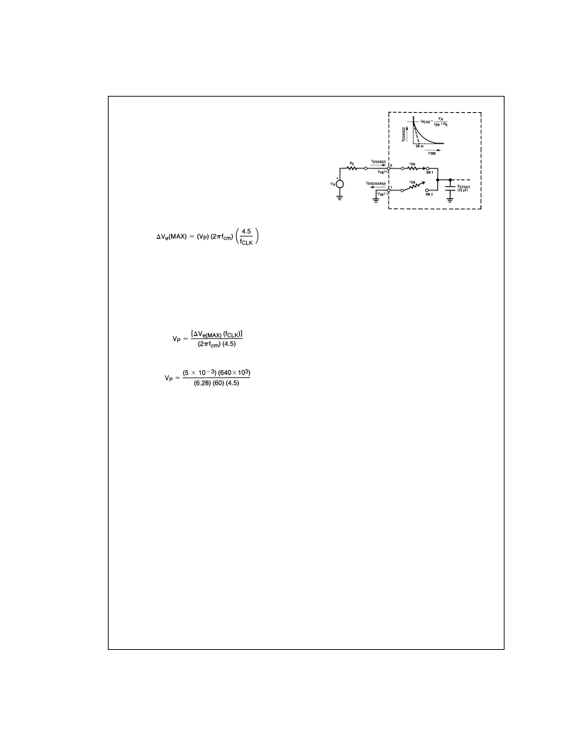
DS005671-14
r
ON
of SW 1 and SW 2
5 k
r=r
ON
C
STRAY
5 k
x 12 pF = 60 ns
FIGURE 5. Analog Input Impedance
A
www.national.com
20
相关PDF资料 |
PDF描述 |
|---|---|
| ADC0804 | 8-Bit, Microprocessor-Compatible A/D Converters |
| ADC08060 | 8-Bit, 20 MSPS to 60 MSPS, 1.3 mW/MSPS A/D Converter |
| ADC08060CIMT | 8-Bit, 20 MSPS to 60 MSPS, 1.3 mW/MSPS A/D Converter |
| ADC0806 | 8-Bit, 20 MSPS to 60 MSPS, 1.3 mW/MSPS A/D Converter |
| ADC08062 | 500 ns A/D Converter with S/H Function and Input Multiplexer |
相关代理商/技术参数 |
参数描述 |
|---|---|
| ADC0802LJ | 制造商:NSC 制造商全称:National Semiconductor 功能描述:8-Bit uP Compatible A/D Converters |
| ADC0802LJ/883 | 制造商:NSC 制造商全称:National Semiconductor 功能描述:8-Bit uP Compatible A/D Converters |
| ADC0802LJ-MIL | 制造商:未知厂家 制造商全称:未知厂家 功能描述:Analog-to-Digital Converter, 8-Bit |
| ADC0803 | 制造商:PHILIPS 制造商全称:NXP Semiconductors 功能描述:CMOS 8-bit A/D converters |
| ADC0803/4-1 | 制造商:未知厂家 制造商全称:未知厂家 功能描述:8-Bit A/D Converter 0-To-70 |
发布紧急采购,3分钟左右您将得到回复。