- 您现在的位置:买卖IC网 > PDF目录378276 > ADC08031CIWM (NATIONAL SEMICONDUCTOR CORP) 8-Bit High-Speed Serial I/O A/D Converters with Multiplexer Options, Voltage Reference, and Track/Hold Function PDF资料下载
参数资料
| 型号: | ADC08031CIWM |
| 厂商: | NATIONAL SEMICONDUCTOR CORP |
| 元件分类: | ADC |
| 英文描述: | 8-Bit High-Speed Serial I/O A/D Converters with Multiplexer Options, Voltage Reference, and Track/Hold Function |
| 中文描述: | 8-CH 8-BIT SUCCESSIVE APPROXIMATION ADC, SERIAL ACCESS, PDSO14 |
| 封装: | SOP-14 |
| 文件页数: | 14/24页 |
| 文件大小: | 509K |
| 代理商: | ADC08031CIWM |
Functional Description
(Continued)
4.0 THE ANALOG INPUTS
The most important feature of these converters is that they
can be located right at the analog signal source and through
just a few wires can communicate with a controlling proces-
sor with a highly noise immune serial bit stream. This in itself
greatly minimizes circuitry to maintain analog signal accu-
racy which otherwise is most susceptible to noise pickup.
However, a few words are in order with regard to the analog
inputs should the input be noisy to begin with or possibly
riding on a large common-mode voltage.
The differential input of these converters actually reduces
the effects of common-mode input noise, a signal common
to both selected “+” and “” inputs for a conversion (60 Hz is
most typical). The time interval between sampling the “+” in-
put and then the “” input is
1
2
of a clock period. The change
in the common-mode voltage during this short time interval
can
cause
conversion
errors.
common-mode signal this error is:
For
a
sinusoidal
where f
CM
is the frequency of the common-mode signal,
V
PEAK
is its peak voltage value
and f
CLK
is the A/D clock frequency.
For a 60Hz common-mode signal to generate a
1
4
LSB error
(
≈
5mV) with the converter running at 250kHz, its peak value
would have to be 6.63V which would be larger than allowed
as it exceeds the maximum analog input limits.
Source resistance limitation is important with regard to the
DC leakage currents of the input multiplexer. Bypass capaci-
tors should not be used if the source resistance is greater
than 1k
. The worst-case leakage current of
±
1μAover tem-
perature will create a 1mV input error with a 1k
source re-
sistance. An op amp RC active low pass filter can provide
both impedance buffering and noise filtering should a high
impedance signal source be required.
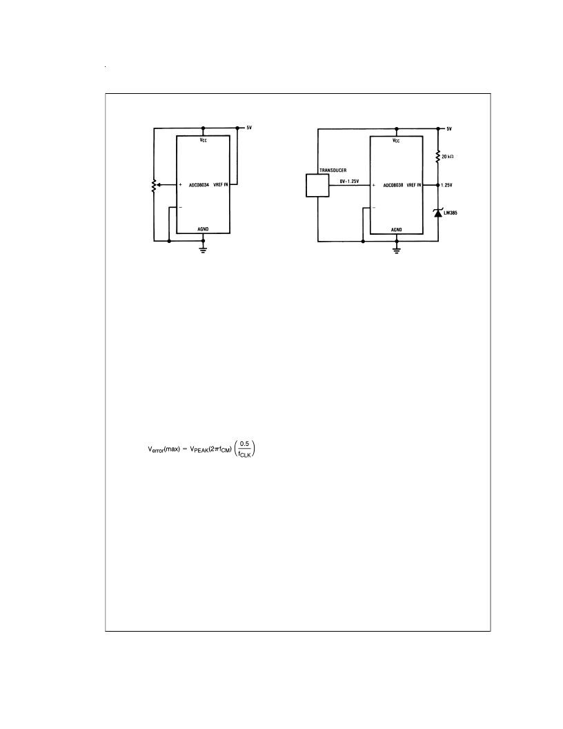
5.0 OPTIONAL ADJUSTMENTS
5.1 Zero Error
The zero of the A/D does not require adjustment. If the mini-
mum analog input voltage value, V
, is not ground a
zero offset can be done. The converter can be made to out-
put 0000 0000 digital code for this minimum input voltage by
biasing any V
() input at this V
value. This utilizes
the differential mode operation of the A/D.
The zero error of the A/D converter relates to the location of
the first riser of the transfer function and can be measured by
grounding the V
() input and applying a small magnitude
positive voltage to the V
(+) input. Zero error is the differ-
ence between the actual DC input voltage which is neces-
sary to just cause an output digital code transition from 0000
0000 to 0000 0001 and the ideal
1
2
LSB value (
1
2
LSB =
9.8mV for V
REF
= 5.000V
DC
).
5.2 Full Scale
The full-scale adjustment can be made by applying a differ-
ential input voltage which is 1
1
2
LSB down from the desired
analog full-scale voltage range and then adjusting the mag-
nitude of the V
IN input for a digital output code which is
just changing from 1111 1110 to 1111 1111.
5.3 Adjusting for an Arbitrary Analog Input
Voltage Range
If the analog zero voltage of the A/D is shifted away from
ground (for example, to accommodate an analog input signal
which does not go to ground), this new zero reference
should be properly adjusted first. A V
IN
(+) voltage which
equals this desired zero reference plus
1
2
LSB (where the
LSB is calculated for the desired analog span, using 1 LSB=
analog span/256) is applied to selected “+” input and the
zero reference voltage at the corresponding “” input should
then be adjusted to just obtain the 00
HEX
to 01
HEX
code tran-
sition.
The full-scale adjustment should be made [with the proper
V
() voltage applied] by forcing a voltage to the V
IN
(+) in-
put which is given by:
DS010555-52
a) Ratiometric
DS010555-53
b) Absolute with a Reduced Span
FIGURE 2. Reference Examples
www.national.com
14
相关PDF资料 |
PDF描述 |
|---|---|
| ADC08034 | 8-Bit High-Speed Serial I/O A/D Converters with Multiplexer Options, Voltage Reference, and Track/Hold Function(8位高速串行输入/输出A/D转换器带多路选择,电压基准和跟踪/保持功能) |
| ADC08038 | 8-Bit High-Speed Serial I/O A/D Converters with Multiplexer Options, Voltage Reference, and Track/Hold Function(8位高速串行输入/输出A/D转换器带多路选择,电压基准和跟踪/保持功能) |
| ADC08034CIWM | 8-Bit High-Speed Serial I/O A/D Converters with Multiplexer Options, Voltage Reference, and Track/Hold Function |
| ADC08032 | 8-Bit High-Speed Serial I/O A/D Converters with Multiplexer Options, Voltage Reference, and Track/Hold Function(8位高速串行输入/输出A/D转换器带多路选择,电压基准和跟踪/保持功能) |
| ADC08032CIWM | 8-Bit High-Speed Serial I/O A/D Converters with Multiplexer Options, Voltage Reference, and Track/Hold Function |
相关代理商/技术参数 |
参数描述 |
|---|---|
| ADC08031CIWM/NOPB | 制造商:Texas Instruments 功能描述:Single ADC SAR 8-bit Serial 14-Pin SOIC W |
| ADC08031CIWMX | 功能描述:IC ADC 8BIT HS SERIAL I/O 14SOIC RoHS:否 类别:集成电路 (IC) >> 数据采集 - 模数转换器 系列:- 产品培训模块:Lead (SnPb) Finish for COTS Obsolescence Mitigation Program 标准包装:2,500 系列:- 位数:12 采样率(每秒):3M 数据接口:- 转换器数目:- 功率耗散(最大):- 电压电源:- 工作温度:- 安装类型:表面贴装 封装/外壳:SOT-23-6 供应商设备封装:SOT-23-6 包装:带卷 (TR) 输入数目和类型:- |
| ADC08031CIWMX/NOPB | 制造商:Texas Instruments 功能描述:ADC Single SAR 8-bit Serial 14-Pin SOIC W T/R |
| ADC08031CMJ | 制造商:未知厂家 制造商全称:未知厂家 功能描述:Analog-to-Digital Converter, 8-Bit |
| ADC0803-1CN | 制造商:PHILIPS 制造商全称:NXP Semiconductors 功能描述:CMOS 8-bit A/D converters |
发布紧急采购,3分钟左右您将得到回复。