- 您现在的位置:买卖IC网 > PDF目录378277 > ADC08034 (National Semiconductor Corporation) 8-Bit High-Speed Serial I/O A/D Converters with Multiplexer Options, Voltage Reference, and Track/Hold Function(8位高速串行输入/输出A/D转换器带多路选择,电压基准和跟踪/保持功能) PDF资料下载
参数资料
| 型号: | ADC08034 |
| 厂商: | National Semiconductor Corporation |
| 元件分类: | 串行ADC |
| 英文描述: | 8-Bit High-Speed Serial I/O A/D Converters with Multiplexer Options, Voltage Reference, and Track/Hold Function(8位高速串行输入/输出A/D转换器带多路选择,电压基准和跟踪/保持功能) |
| 中文描述: | 8位高速串行I /办公自动化/ D的多路复用器选项,电压参考,并跟踪转换器/保持功能(8位高速串行输入/输出的A / D转换器带多路选择,电压基准和跟踪/保持功能) |
| 文件页数: | 14/24页 |
| 文件大小: | 552K |
| 代理商: | ADC08034 |
Functional Description
(Continued)
3.0 REFERENCE CONSIDERATIONS
The voltage applied to the reference input on these convert-
ers, V
IN, defines the voltage span of the analog input
(the difference between V
and V
over which the
256 possible output codes apply. The devices can be used
either in ratiometric applications or in systems requiring ab-
solute accuracy. The reference pin must be connected to a
voltage source capable of driving the reference input resis-
tance which can be as low as 1.3k
. This pin is the top of a
resistor divider string and capacitor array used for the suc-
cessive approximation conversion.
In a ratiometric system the analog input voltage is propor-
tional to the voltage used for the A/D reference. This voltage
is typically the system power supply, so the V
IN pin can
be tied to V
(done internally on the ADC08032). This tech-
nique relaxes the stability requirements of the system refer-
ence as the analog input and A/D reference move together
maintaining the same output code for a given input condition.
For absolute accuracy, where the analog input varies be-
tween very specific voltage limits, the reference pin can be
biased with a time and temperature stable voltage source.
For the ADC08034 and the ADC08038 a band-gap derived
reference voltage of 2.6V (Note 8) is tied to V
REF
OUT. This
can be tied back to V
REF
IN. Bypassing V
REF
OUT with a
100μF capacitor is recommended. The LM385 and LM336
reference diodes are good low current devices to use with
these converters.
The maximum value of the reference is limited to the V
supply voltage. The minimum value, however, can be quite
small (see Typical Performance Characteristics) to allow di-
rect conversions of transducer outputs providing less than a
5V output span. Particular care must be taken with regard to
noise pickup, circuit layout and system error voltage sources
when operating with a reduced span due to the increased
sensitivity of the converter (1 LSB equals V
REF/
256).
4.0 THE ANALOG INPUTS
The most important feature of these converters is that they
can be located right at the analog signal source and through
just a few wires can communicate with a controlling proces-
sor with a highly noise immune serial bit stream. This in itself
greatly minimizes circuitry to maintain analog signal accu-
racy which otherwise is most susceptible to noise pickup.
However, a few words are in order with regard to the analog
inputs should the input be noisy to begin with or possibly
riding on a large common-mode voltage.
The differential input of these converters actually reduces
the effects of common-mode input noise, a signal common
to both selected “+” and “” inputs for a conversion (60 Hz is
most typical). The time interval between sampling the “+” in-
put and then the “” input is
1
2
of a clock period. The change
in the common-mode voltage during this short time interval
can
cause
conversion
errors.
common-mode signal this error is:
For
a
sinusoidal
where f
CM
is the frequency of the common-mode signal,
V
PEAK
is its peak voltage value
and f
CLK
is the A/D clock frequency.
For a 60Hz common-mode signal to generate a
1
4
LSB error
(
≈
5mV) with the converter running at 250kHz, its peak value
would have to be 6.63V which would be larger than allowed
as it exceeds the maximum analog input limits.
Source resistance limitation is important with regard to the
DC leakage currents of the input multiplexer. Bypass capaci-
tors should not be used if the source resistance is greater
than 1k
. The worst-case leakage current of
±
1μAover tem-
perature will create a 1mV input error with a 1k
source re-
sistance. An op amp RC active low pass filter can provide
both impedance buffering and noise filtering should a high
impedance signal source be required.
5.0 OPTIONAL ADJUSTMENTS
5.1 Zero Error
The zero of the A/D does not require adjustment. If the mini-
mum analog input voltage value, V
, is not ground a
zero offset can be done. The converter can be made to out-
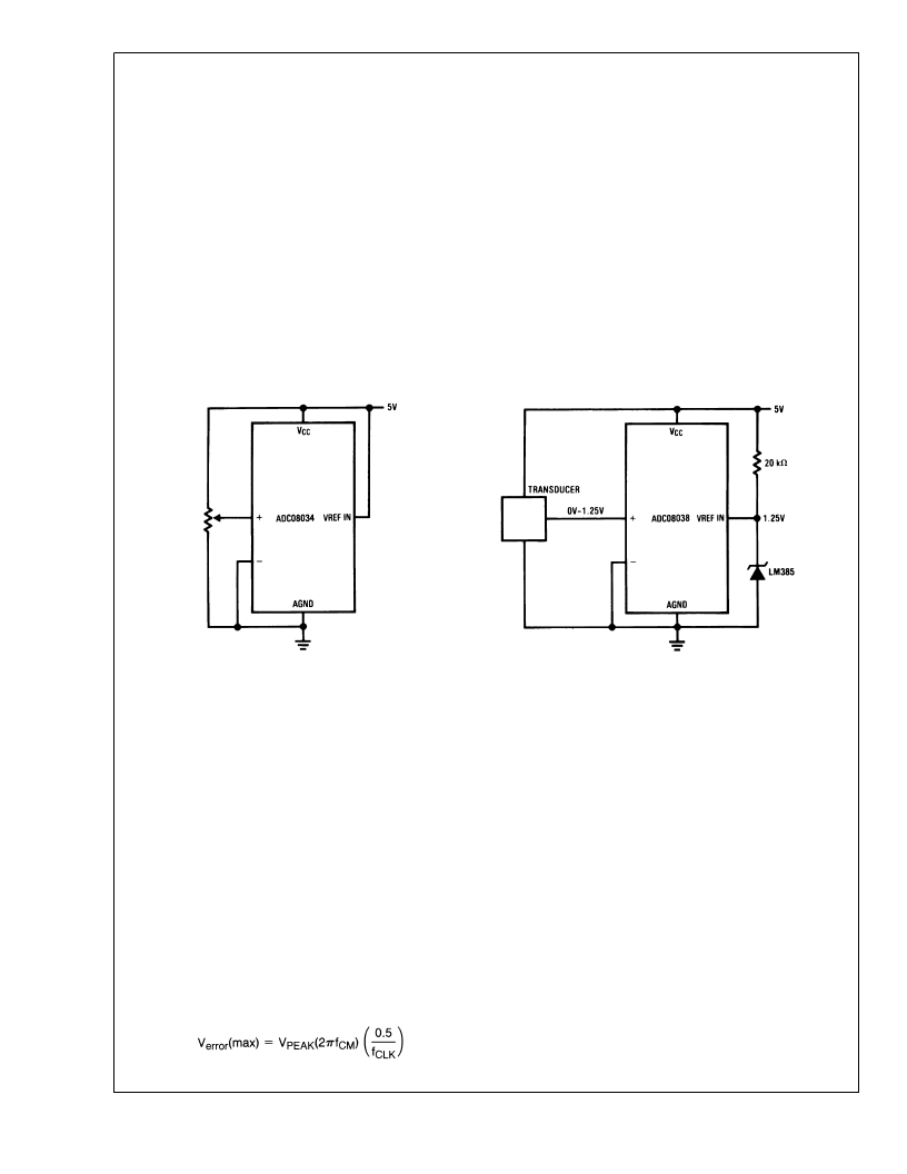
DS010555-52
a) Ratiometric
DS010555-53
b) Absolute with a Reduced Span
FIGURE 2. Reference Examples
A
www.national.com
14
相关PDF资料 |
PDF描述 |
|---|---|
| ADC08038 | 8-Bit High-Speed Serial I/O A/D Converters with Multiplexer Options, Voltage Reference, and Track/Hold Function(8位高速串行输入/输出A/D转换器带多路选择,电压基准和跟踪/保持功能) |
| ADC08034CIWM | 8-Bit High-Speed Serial I/O A/D Converters with Multiplexer Options, Voltage Reference, and Track/Hold Function |
| ADC08032 | 8-Bit High-Speed Serial I/O A/D Converters with Multiplexer Options, Voltage Reference, and Track/Hold Function(8位高速串行输入/输出A/D转换器带多路选择,电压基准和跟踪/保持功能) |
| ADC08032CIWM | 8-Bit High-Speed Serial I/O A/D Converters with Multiplexer Options, Voltage Reference, and Track/Hold Function |
| ADC08038CIWM | 8-Bit High-Speed Serial I/O A/D Converters with Multiplexer Options, Voltage Reference, and Track/Hold Function |
相关代理商/技术参数 |
参数描述 |
|---|---|
| ADC08034BIJ | 制造商:未知厂家 制造商全称:未知厂家 功能描述:Single-Ended Data Acquisition System |
| ADC08034BIN | 制造商:未知厂家 制造商全称:未知厂家 功能描述:Single-Ended Data Acquisition System |
| ADC08034CIJ | 制造商:未知厂家 制造商全称:未知厂家 功能描述:Single-Ended Data Acquisition System |
| ADC08034CIWM | 制造商:Rochester Electronics LLC 功能描述:8-BIT 8US SERIAL, 4-CH MUX - Bulk 制造商:Texas Instruments 功能描述: |
| ADC08034CIWMX | 功能描述:IC ADC 8BIT HS SERIAL I/O 14SOIC RoHS:否 类别:集成电路 (IC) >> 数据采集 - 模数转换器 系列:- 产品培训模块:Lead (SnPb) Finish for COTS Obsolescence Mitigation Program 标准包装:2,500 系列:- 位数:12 采样率(每秒):3M 数据接口:- 转换器数目:- 功率耗散(最大):- 电压电源:- 工作温度:- 安装类型:表面贴装 封装/外壳:SOT-23-6 供应商设备封装:SOT-23-6 包装:带卷 (TR) 输入数目和类型:- |
发布紧急采购,3分钟左右您将得到回复。