- 您现在的位置:买卖IC网 > PDF目录378277 > ADC0805 (National Semiconductor Corporation) 8-Bit uP Compatible A/D Converters PDF资料下载
参数资料
| 型号: | ADC0805 |
| 厂商: | National Semiconductor Corporation |
| 元件分类: | 串行ADC |
| 英文描述: | 8-Bit uP Compatible A/D Converters |
| 中文描述: | 8位的兼容的A / D转换器 |
| 文件页数: | 18/41页 |
| 文件大小: | 1118K |
| 代理商: | ADC0805 |
第1页第2页第3页第4页第5页第6页第7页第8页第9页第10页第11页第12页第13页第14页第15页第16页第17页当前第18页第19页第20页第21页第22页第23页第24页第25页第26页第27页第28页第29页第30页第31页第32页第33页第34页第35页第36页第37页第38页第39页第40页第41页
Functional Description
(Continued)
2.0 FUNCTIONAL DESCRIPTION
The ADC0801 series contains a circuit equivalent of the
256R network. Analog switches are sequenced by succes-
sive approximation logic to match the analog difference input
voltage [V
(+) V
()] to a corresponding tap on the R net-
work. The most significant bit is tested first and after 8 com-
parisons (64 clock cycles) a digital 8-bit binary code (1111
1111 = full-scale) is transferred to an output latch and then
an interrupt is asserted (INTR makes a high-to-low transi-
tion).Aconversion in process can be interrupted by issuing a
second start command. The device may be operated in the
free-running mode by connecting INTR to the WR input with
CS =0. To ensure start-up under all possible conditions, an
external WR pulse is required during the first power-up
cycle.
On the high-to-low transition of the WR input the internal
SAR latches and the shift register stages are reset. As long
as the CS input and WR input remain low, theA/D will remain
in a reset state. Conversion will start from 1 to 8 clock peri-
ods after at least one of these inputs makes a low-to-high
transition
A functional diagram of the A/D converter is shown in Figure
4 All of the package pinouts are shown and the major logic
control paths are drawn in heavier weight lines.
The converter is started by having CS and WR simulta-
neously low. This sets the start flip-flop (F/F) and the result-
ing “1” level resets the 8-bit shift register, resets the Interrupt
(INTR) F/F and inputs a “1” to the D flop, F/F1, which is at the
input end of the 8-bit shift register. Internal clock signals then
transfer this “1” to the Q output of F/F1. The AND gate, G1,
combines this “1” output with a clock signal to provide a reset
signal to the start F/F. If the set signal is no longer present
(either WR or CS is a “1”) the start F/F is reset and the 8-bit
shift register then can have the “1” clocked in, which starts
the conversion process. If the set signal were to still be
present, this reset pulse would have no effect (both outputs
of the start F/F would momentarily be at a “1” level) and the
8-bit shift register would continue to be held in the reset
mode. This logic therefore allows for wide CS and WR sig-
nals and the converter will start after at least one of these
signals returns high and the internal clocks again provide a
reset signal for the start F/F.
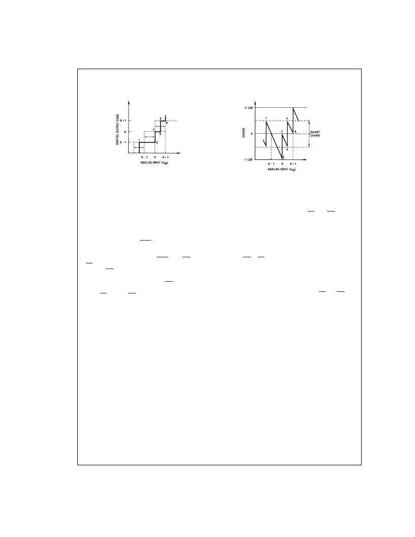
Transfer Function
DS005671-85
Error Plot
DS005671-86
FIGURE 3. Clarifying the Error Specs of an A/D Converter
Accuracy=
±
1
2
LSB
A
www.national.com
18
相关PDF资料 |
PDF描述 |
|---|---|
| ADC0802LCWM | 8-Bit uP Compatible A/D Converters |
| ADC0801LCN | 8-Bit uP Compatible A/D Converters |
| ADC0802 | 8-Bit, Microprocessor- Compatible, A/D Converters |
| ADC0802LCD | 8-Bit, Microprocessor- Compatible, A/D Converters |
| ADC0802LCN | 8-Bit, Microprocessor- Compatible, A/D Converters |
相关代理商/技术参数 |
参数描述 |
|---|---|
| ADC0805CN | 制造商:未知厂家 制造商全称:未知厂家 功能描述:Analog-to-Digital Converter, 8-Bit |
| ADC0805IN | 制造商:未知厂家 制造商全称:未知厂家 功能描述:Analog-to-Digital Converter, 8-Bit |
| ADC0805LCN | 制造商:OC White Company 功能描述:ADC Single SAR 8-bit Parallel 20-Pin PDIP Rail |
| ADC0805LCN/A+ | 制造商:未知厂家 制造商全称:未知厂家 功能描述:Analog-to-Digital Converter, 8-Bit |
| ADC0805LCN/B+ | 制造商:未知厂家 制造商全称:未知厂家 功能描述:Analog-to-Digital Converter, 8-Bit |
发布紧急采购,3分钟左右您将得到回复。