- 您现在的位置:买卖IC网 > PDF目录378277 > ADC08060CIMT (NATIONAL SEMICONDUCTOR CORP) 8-Bit, 20 MSPS to 60 MSPS, 1.3 mW/MSPS A/D Converter PDF资料下载
参数资料
| 型号: | ADC08060CIMT |
| 厂商: | NATIONAL SEMICONDUCTOR CORP |
| 元件分类: | ADC |
| 英文描述: | 8-Bit, 20 MSPS to 60 MSPS, 1.3 mW/MSPS A/D Converter |
| 中文描述: | 1-CH 8-BIT RESISTANCE LADDER ADC, PARALLEL ACCESS, PDSO24 |
| 封装: | PLASTIC, TSSOP-24 |
| 文件页数: | 17/19页 |
| 文件大小: | 539K |
| 代理商: | ADC08060CIMT |
Applications Information
(Continued)
4.0 THE DIGITAL INPUT PINS
The ADC08060 has two digital input pins: The PD pin and
the Clock pin.
4.1 The PD Pin
The Power Down (PD) pin, when high, puts the ADC08060
into a low power mode where power consumption is reduced
to 1 mW. Output data is valid and accurate about 1 millisec-
ond after the PD pin is brought low.
The digital output pins retain the last conversion output code
when either the clock is stopped or the PD pin is high.
4.2 The ADC08060 Clock
Although the ADC08060 is tested and its performance is
guaranteed with a 60 MHz clock, it typically will function well
with clock frequencies from 20 MHz to 70 MHz.
Halting the clock will provide nearly as much power saving
as raising the PD pin high. Typical power consumption with a
stopped clock is 3 mW, compared to 1 mW when PD is high.
The digital outputs will remain in the same state as they were
before the clock was halted.
Once the clock is restored (or the PD pin is brought low),
there is a time of 2.5 clock cycles plus t
OD
before the output
data is valid. However, because of the linear relationship
between total power consumption and clock frequency, the
part requires several microseconds after the clock is re-
started or substantially changed in frequency before the part
returns to its specified accuracy.
The low and high times of the clock signal can affect the
performance of any A/D Converter. Because achieving a
precise duty cycle is difficult, the ADC08060 is designed to
maintain performance over a range of duty cycles. While it is
specified and performance is guaranteed with a 50% clock
duty cycle and 60 Msps, ADC08060 performance is typically
maintained with clock high and low times of 6.7 ns, corre-
sponding to a clock duty cycle range of 40% to 50% with a
60 MHz clock.
The
CLOCK
line should be series terminated at the clock
source in the characteristic impedance of that line. If the
clock line is longer than
where t
r
is the clock rise time and t
is the propagation rate
of the signal along the trace, the
CLOCK
pin should be a.c.
terminated with a series RC to ground such that the resistor
value is equal to the characteristic impedance of the clock
line and the capacitor value is
where t
PD
is the signal propagation rate down the clock line,
"L" is the line length and Z
o
is the characteristic impedance
of the clock line. This termination should be located as close
as possible to, but within one centimeter of, the ADC08060
clock pin. Typical t
PD
is about 150 ps/inch on FR-4 board
material. For FR-4 board material, the value of C becomes
where L is the length of the clock line in inches.
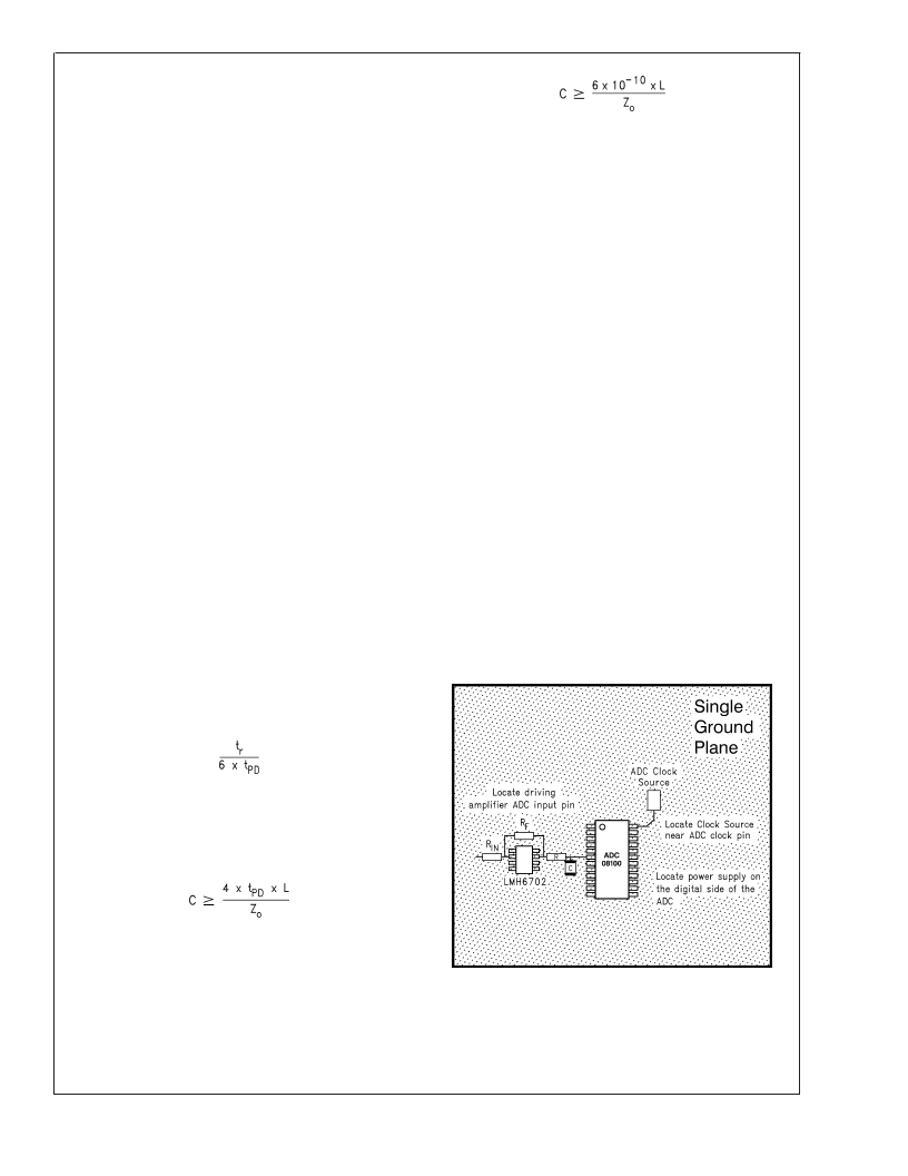
5.0 LAYOUT AND GROUNDING
Proper grounding and proper routing of all signals are es-
sential to ensure accurate conversion. A combined analog
and digital ground plane should be used.
Since digital switching transients are composed largely of
high frequency components, total ground plane copper
weight will have little effect upon the logic-generated noise
because of the skin effect. Total surface area is more impor-
tant than is total ground plane volume. Capacitive coupling
between the typically noisy digital circuitry and the sensitive
analog circuitry can lead to poor performance that may seem
impossible to isolate and remedy. The solution is to keep the
analog circuitry well separated from the digital circuitry.
High power digital components should not be located on or
near a straight line between the ADC (or any linear compo-
nent) and the power supply area as the resulting common
return current path could cause fluctuation in the analog
“ground” return of the ADC.
Generally, analog and digital lines should cross each other at
90 to avoid getting digital noise into the analog path. In high
frequency systems, however, avoid crossing analog and
digital lines altogether. Clock lines should be isolated from
ALL other lines, analog AND digital. Even the generally
accepted 90 crossing should be avoided as even a little
coupling can cause problems at high frequencies. Best per-
formance at high frequencies is obtained with a straight
signal path.
The analog input should be isolated from noisy signal traces
to avoid coupling of spurious signals into the input. Any
external component (e.g., a filter capacitor) connected be-
tween the converter’s input and ground should be connected
to a very clean point in the analog ground plane.
20006236
FIGURE 5. Layout Example
A
www.national.com
17
相关PDF资料 |
PDF描述 |
|---|---|
| ADC0806 | 8-Bit, 20 MSPS to 60 MSPS, 1.3 mW/MSPS A/D Converter |
| ADC08062 | 500 ns A/D Converter with S/H Function and Input Multiplexer |
| ADC08061 | 500 ns A/D Converter with S/H Function and Input Multiplexer |
| ADC08061BIN | TIMER DIGITAL LED RoHS Compliant: Yes |
| ADC08062BIN | 500 ns A/D Converter with S/H Function and Input Multiplexer |
相关代理商/技术参数 |
参数描述 |
|---|---|
| ADC08060CIMT/NOPB | 功能描述:模数转换器 - ADC RoHS:否 制造商:Texas Instruments 通道数量:2 结构:Sigma-Delta 转换速率:125 SPs to 8 KSPs 分辨率:24 bit 输入类型:Differential 信噪比:107 dB 接口类型:SPI 工作电源电压:1.7 V to 3.6 V, 2.7 V to 5.25 V 最大工作温度:+ 85 C 安装风格:SMD/SMT 封装 / 箱体:VQFN-32 |
| ADC08060CIMT/NOPB | 制造商:Texas Instruments 功能描述:A/D Converter (A-D) IC |
| ADC08060CIMTX | 功能描述:模数转换器 - ADC RoHS:否 制造商:Texas Instruments 通道数量:2 结构:Sigma-Delta 转换速率:125 SPs to 8 KSPs 分辨率:24 bit 输入类型:Differential 信噪比:107 dB 接口类型:SPI 工作电源电压:1.7 V to 3.6 V, 2.7 V to 5.25 V 最大工作温度:+ 85 C 安装风格:SMD/SMT 封装 / 箱体:VQFN-32 |
| ADC08060CIMTX/NOPB | 功能描述:模数转换器 - ADC RoHS:否 制造商:Texas Instruments 通道数量:2 结构:Sigma-Delta 转换速率:125 SPs to 8 KSPs 分辨率:24 bit 输入类型:Differential 信噪比:107 dB 接口类型:SPI 工作电源电压:1.7 V to 3.6 V, 2.7 V to 5.25 V 最大工作温度:+ 85 C 安装风格:SMD/SMT 封装 / 箱体:VQFN-32 |
| ADC08060EVAL | 制造商:NSC 制造商全称:National Semiconductor 功能描述:8-Bit, 20 MSPS to 60 MSPS, 1.3 mW/MSPS A/D Converter with Internal Sample-and-Hold |
发布紧急采购,3分钟左右您将得到回复。